Focal plane array processing method and apparatus

a processing method and array technology, applied in the field of focal plane array processing, can solve the problems of not being able to meet the above requirements in combination, not being able to meet the above requirements, and being unable to meet the requirements of specific analog designs,

Active Publication Date: 2012-06-07
MASSACHUSETTS INST OF TECH
View PDF3 Cites 50 Cited by
  • Summary
  • Abstract
  • Description
  • Claims
  • Application Information

AI Technical Summary

Problems solved by technology

Conventional FPAs are not particularly well suited to satisfying combinations of the above requirements.
Specific analog designs can target (and possibly satisfy) one or more requirement, but fail when simultaneously targeting the most aggressive design parameters for imaging applications, such as long-wave infrared imaging (LWIR) applications.
Fundamental limitations on achievable well depth (with concomitant limitations on capacitor size), and the readout noise floor, limit practical scalability of conventional designs.
Capacitor size limitations require unnecessarily high frame rates to avoid saturating pixels.
Attempting to scale conventional analog technology to meet the most demanding requirements leads to a high-power-consumption FPA with many data output taps.
This in turn leads to a large, massive, and complex sensor system.

Method used


Image

  • Focal plane array processing method and apparatus
  • Focal plane array processing method and apparatus
  • Focal plane array processing method and apparatus

Examples


Embodiment Construction

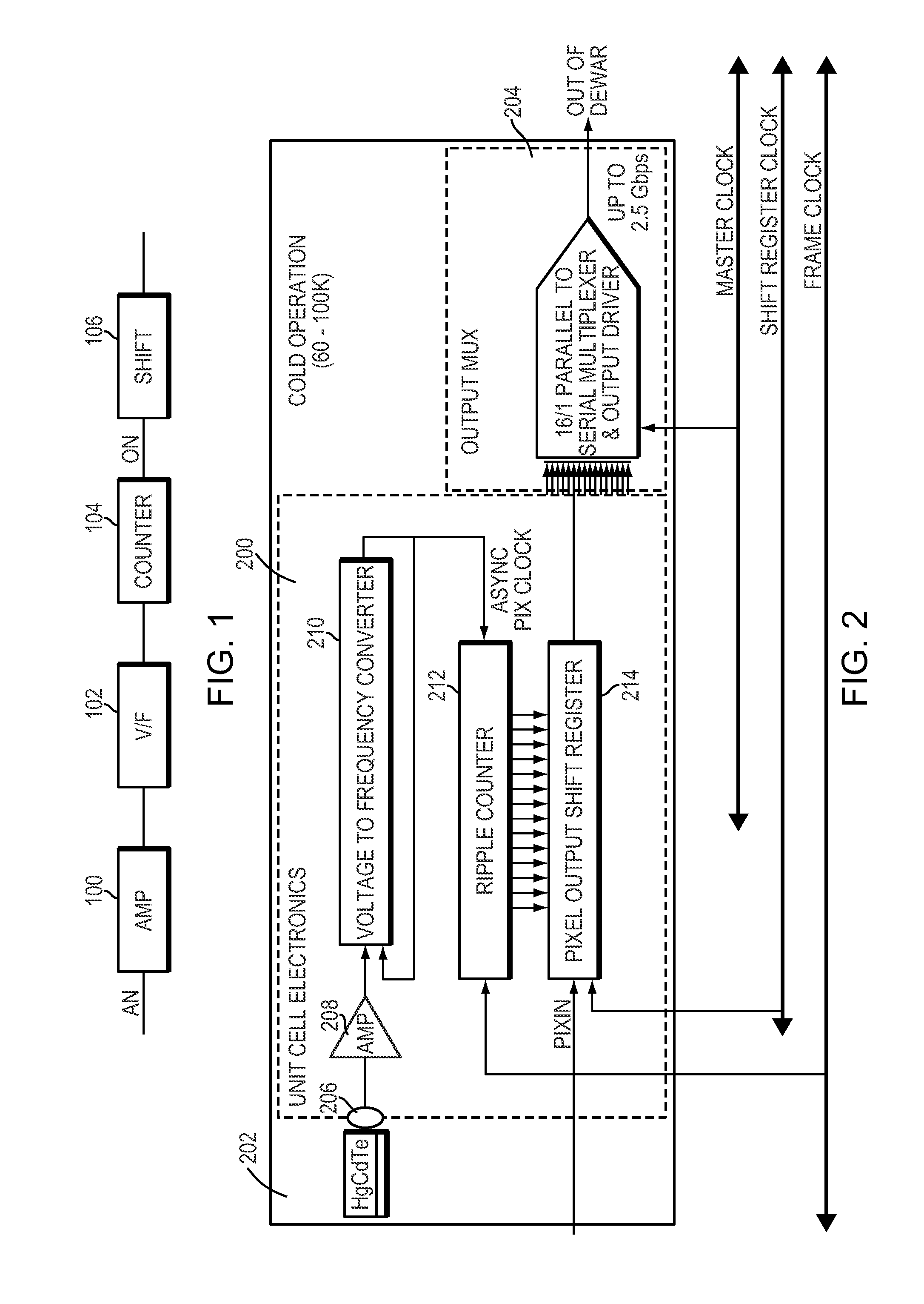
[0043]The block diagram of FIG. 1 illustrates the major components of an individual ADC, such as may be found employed within a focal plane sensor array in accordance with the principles of the present invention. An amplifier 100 (which is optional, depending upon the quality of the signal to be converted) accepts an analog signal, AN, for conversion, amplifies and conditions the signal, AN, and provides the conditioned signal to a voltage to frequency converter (V-to-F) 102. In illustrative embodiments the amplifier 100 may be a direct injection, buffered direct injection, source-follower, or transimpedance amplifier, for example. The voltage-to-frequency converter 102 converters the voltage signal from the amplifier to a serial digital signal, the frequency of which is representative of the voltage input. The digital output of the voltage-to-frequency converter is routed to a counter 104, where the digital stream is counted. The resulting count, DN, is a digital signal the magnitu...


PUM


Abstract

A digital focal plane array includes an all-digital readout integrated circuit in combination with a detector array. The readout circuit includes unit cell electronics, orthogonal transfer structures, and data handling structures. The unit cell electronics include an analog to digital converter. Orthogonal transfer structures enable the orthogonal transfer of data among the unit cells. Data handling structures may be configured to operate the digital focal plane array as a data encryptor / decipherer. Data encrypted and deciphered by the digital focal plane array need not be image data.

Description

RELATED APPLICATIONS[0001]This application is a divisional application of Ser. No. 11 / 978,351, filed on Oct. 29, 2007, entitled “Focal Plane Array Processing Method and Apparatus,” which claims a priority benefit under 35 U.S.C. §119(e) of U.S. provisional application No. 60 / 854,963 entitled FOCAL PLANE ARRAY FOR ON-CHIP DATA PROCESSING, filed Oct. 27, 2006. Each of the above-referenced applications is incorporated herein by reference in its entirety.GOVERNMENT SUPPORT[0002]This invention was made with government support under U.S. Air Force contract FA8721-05-C-0002. The government has certain rights in this invention.FIELD OF THE INVENTION[0003]The invention relates to focal plane arrays and, in particular, to signal processing focal plane arrays.BACKGROUND OF THE INVENTION[0004]High performance focal plane array (FPA) applications require wide-area coverage, high signal-to-noise-ratios (SNR), high spatial resolution, and high frame rates in various combinations. Conventional FPAs...

Claims


Application Information

Patent Timeline
Patent Type & Authority Applications(United States)
IPC IPC(8): H01L27/146
CPCG11B20/00086G11B20/0021H04N5/33H04N5/378H04N5/772H04N5/913H04L2209/805H04N21/4408H04N2005/91364G09C1/00H04L2209/12H04L9/0637H04L9/12H04N21/4223H04N25/75G06F21/602H04L9/0631
Inventor KELLY, MICHAELTYRRELL, BRIANCOLONERO, CURTISBERGER, ROBERTSCHULTZ, KENNETHWEY, JAMESMOONEY, DANIELCANDELL, LAWRENCE
Owner MASSACHUSETTS INST OF TECH
Why Eureka
Try Eureka