Semiconductor device having metal gate and manufacturing method thereof

a technology of metal gate and semiconductor device, which is applied in the direction of semiconductor device, electrical apparatus, transistor, etc., can solve the problems of deteriorating electrical performance of the transistor device having the metal gate, seam left in the metal gate, and reduced opening width of the gate trench, so as to improve reliability, facilitate formation, and improve the effect of gap-filling results

Active Publication Date: 2012-06-07
MARLIN SEMICON LTD
View PDF4 Cites 21 Cited by
  • Summary
  • Abstract
  • Description
  • Claims
  • Application Information

AI Technical Summary

Benefits of technology

[0009]According to the semiconductor device having a metal gate and the method of manufacturing a semiconductor device having metal gate provided by the present invention, the T-shaped gate trench constructed by the first recess and the second recess is obtained by performing two etching processes. According to the present invention, the T-shaped gate trench includes a larger opening width, thus the metal layers are easily formed in the trench gate. Consequently, the semiconductor device having metal gate provided by the present invention has the advantage of superior gap-filling result and improved reliability.

Problems solved by technology

Briefly speaking, when the line width of the transistor device is reduced, the opening width of the gate trench is consequently reduced, and thus it is difficult to fill the gate trench with the metals, it even causes a seam left in the metal gate after forming the metal layers in the gate trench.
Eventually, the electrical performance of the transistor device having the metal gate is deteriorated.
However, the gate last process still faces integrity requirements for the complicated processes and reliability requirement for the gate trench filling.

Method used


Image

  • Semiconductor device having metal gate and manufacturing method thereof
  • Semiconductor device having metal gate and manufacturing method thereof
  • Semiconductor device having metal gate and manufacturing method thereof

Examples


Embodiment Construction

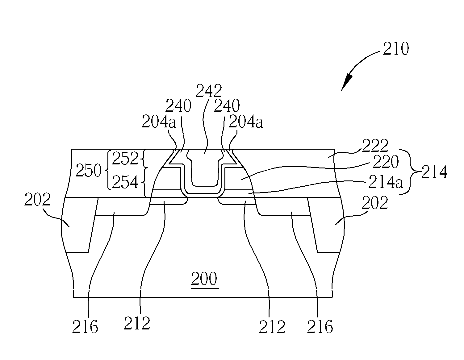
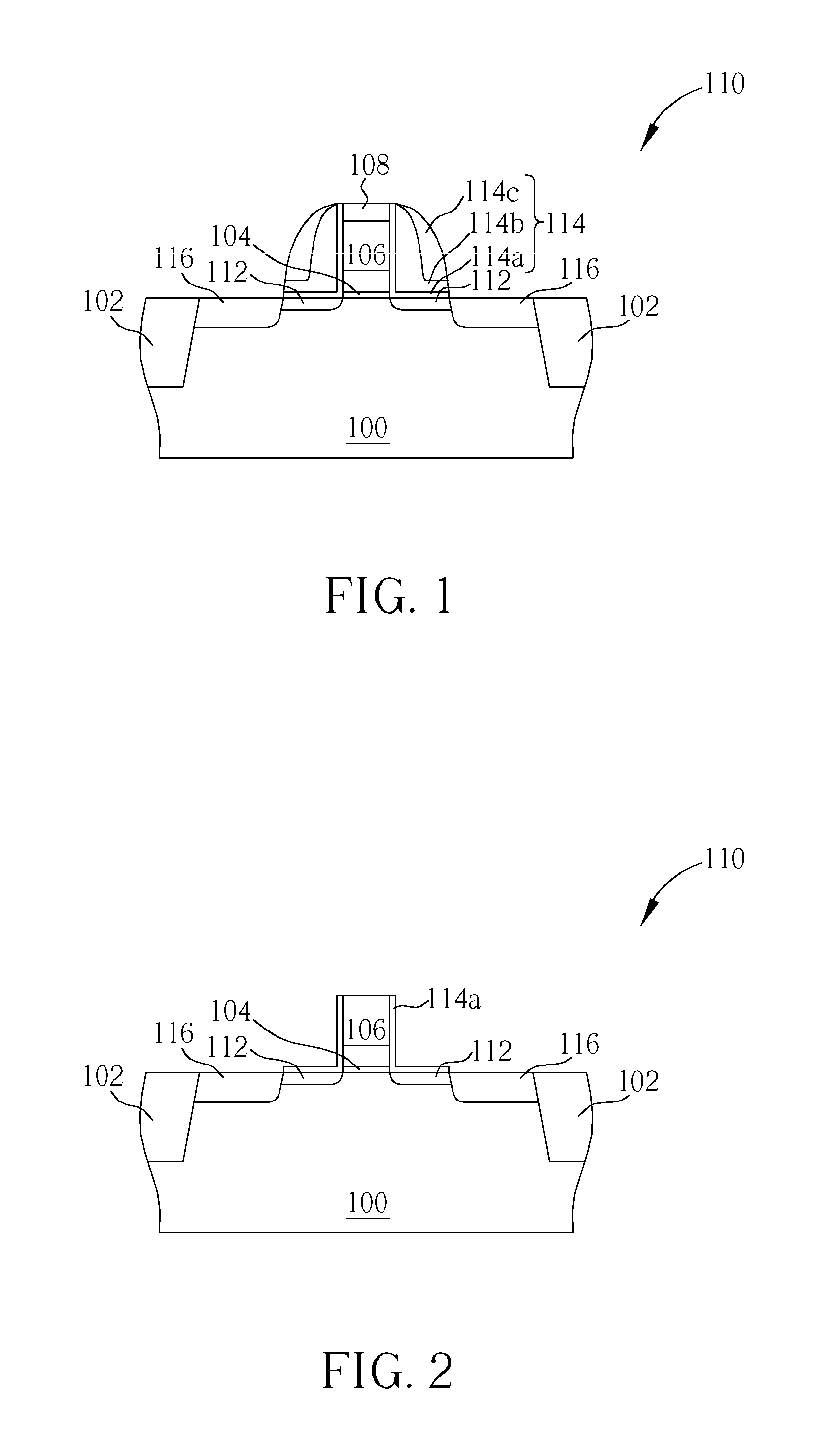
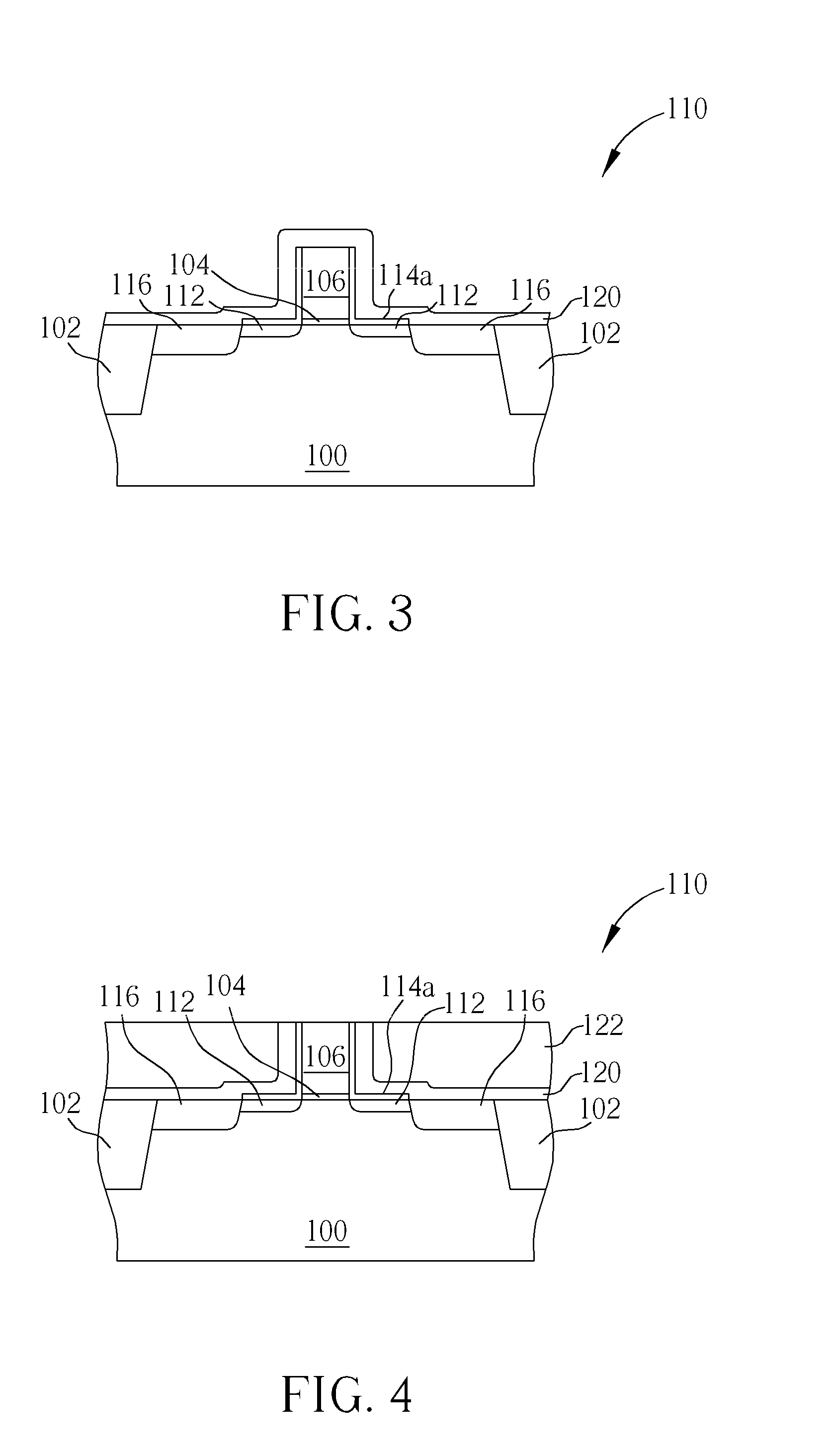
[0013]Please refer to FIGS. 1-8, which are schematic drawings illustrating a method of manufacturing a semiconductor device having metal gate provided by a first preferred embodiment of the present invention. As shown in FIG. 1, a substrate 100 such as a silicon substrate, a silicon-containing substrate, or a silicon-on-insulator (SOI) substrate is provided. A plurality of shallow trench isolation (STI) 102 is formed in the substrate 100 for providing electrical isolation. Subsequently, at least a semiconductor device 110 is formed on the substrate 100. The semiconductor device 110 includes a gate dielectric layer 104, a dummy gate 106 such as a polysilicon layer, and a patterned hard mask 108. The gate dielectric layer 104 can be a conventional SiO layer or a high-K gate dielectric layer. It is noteworthy that when a high-K first process is integrated into the preferred embodiment, the gate dielectric layer 104 includes a high-K gate dielectric layer, and the high-K gate dielectric...


PUM


Abstract

A method of manufacturing a semiconductor device having metal gate includes providing a substrate having at least a dummy gate, a sacrificial layer covering sidewalls of the dummy gate and a dielectric layer exposing a top of the dummy gate formed thereon, forming a sacrificial layer covering sidewalls of the dummy gate on the substrate, forming a dielectric layer exposing a top of the dummy gate on the substrate, performing a first etching process to remove a portion of the sacrificial layer surrounding the top of the dummy gate to form at least a first recess, and performing a second etching process to remove the dummy gate to form a second recess. The first recess and the second recess construct a T-shaped gate trench.

Description

BACKGROUND OF THE INVENTION[0001]1. Field of the Invention[0002]The invention relates to a semiconductor device having a metal gate and manufacturing method thereof, and more particularly, to a semiconductor device having a metal gate and manufacturing method applied with a gate last process.[0003]2. Description of the Prior Art[0004]With a trend toward scaling down the size of the semiconductor device, work function metals are used to replace the conventional polysilicon gate to be the control electrode that competent to the high-K gate dielectric layer. The conventional dual metal gate methods are categorized into the gate first process and the gate last process. Among the two main approaches, the gate last process is able to avoid processes of high thermal budget and to provide wider material choices for the high-K gate dielectric layer and the metal gate, and thus gradually replaces the gate first process.[0005]In a conventional gate last process, a dummy gate or a replacement g...

Claims


Application Information

Patent Timeline
Patent Type & Authority Applications(United States)
IPC IPC(8): H01L21/336H01L29/78
CPCH01L21/28114H01L29/42376H01L29/6653H01L29/66492H01L29/6659H01L29/7833H01L29/7843H01L29/66545
Inventor FU, SSU-ITSENG, I-MINGLIOU, EN-CHIUANCHEN, CHENG-GUO
Owner MARLIN SEMICON LTD
Why Eureka
Try Eureka