
Optical memory device based on dhlfc material and method of preparing the same

a memory device and optical memory technology, applied in the direction of digital storage, lamination ancillary operations, instruments, etc., can solve the problems of poor repeatability in such cells, costlier gnps, difficult dispersion,

Inactive Publication Date: 2012-06-07
COUNCIL OF SCI & IND RES
View PDF2 Cites 2 Cited by
  • Summary
  • Abstract
  • Description
  • Claims
  • Application Information

AI Technical Summary

Benefits of technology

[0016]The main object of the present invention is to provide a long duration optical memory device based on glycerol mixed deformed helix ferroelectric liquid crystal material having applications in ferroelectric liquid crystal based devices, which obviate the drawbacks of hitherto known memory devices based on other types of liquid crystal materials.
[0018]Yet another object of the present invention is to provide an optical memory device having faster response.

Problems solved by technology

The drawbacks of the memory devices based on above principle are stability and a uniform alignment over a large area because of the difficulty in applying uniform shear and to maintain a uniform temperature through out the SSFLC display.
The technique thus cannot be used as a commercially viable one.
But the GNPs are costlier and difficult to disperse in LC, and so, the repeatability is poor in such cells.
But CNTs are very difficult to synthesize and very difficult to disperse homogeneously in liquid crystal material.

Method used

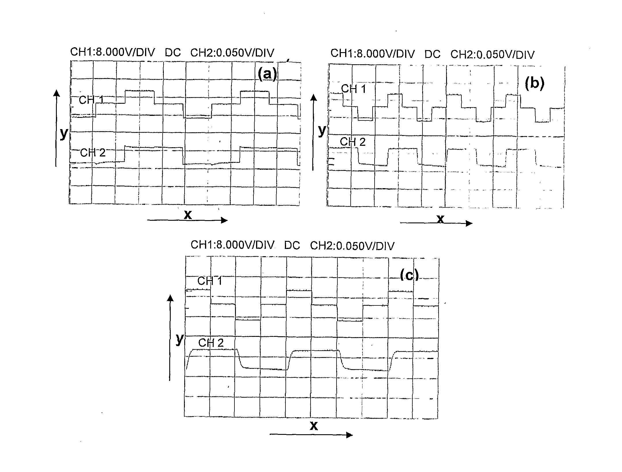
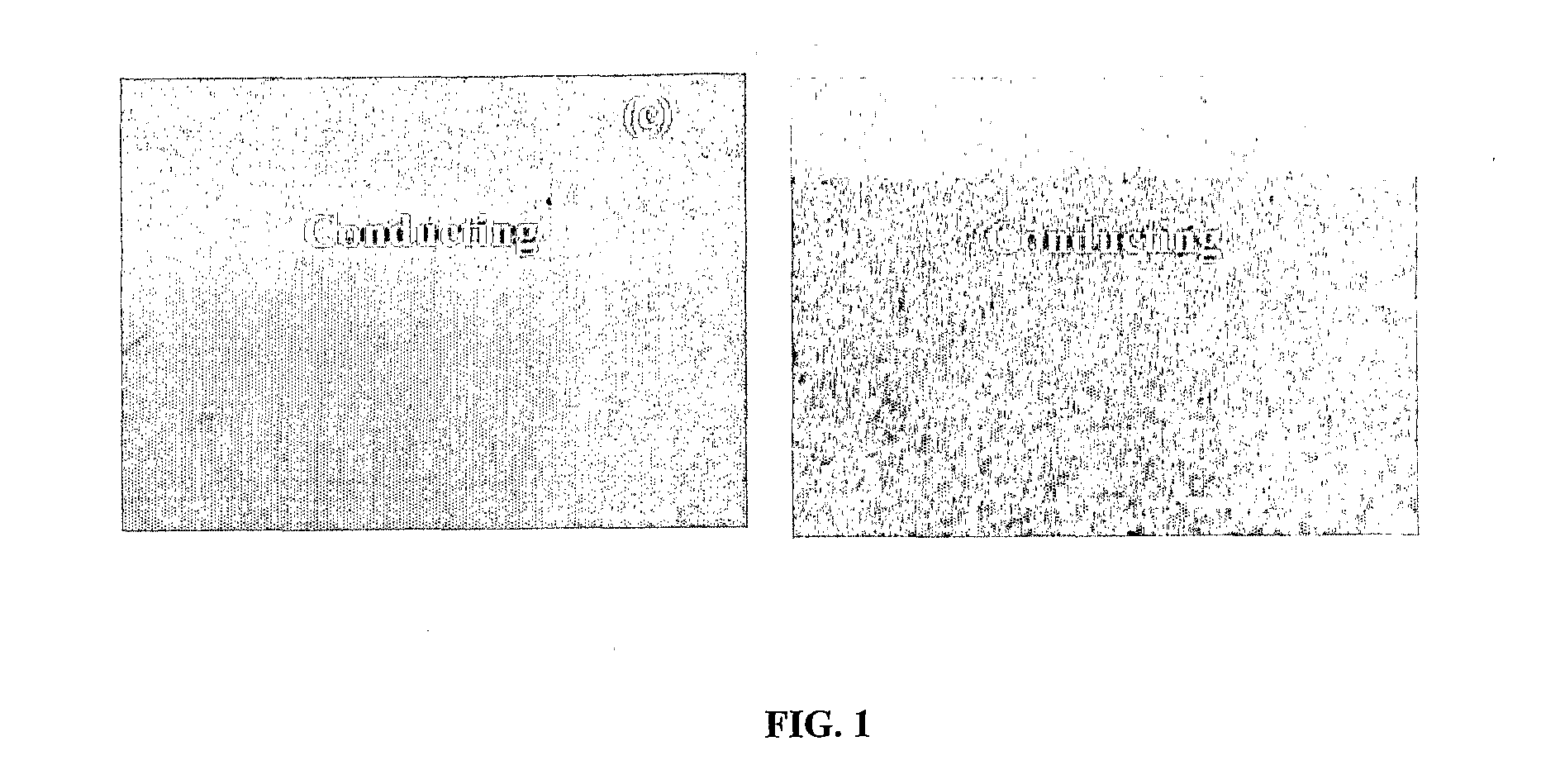
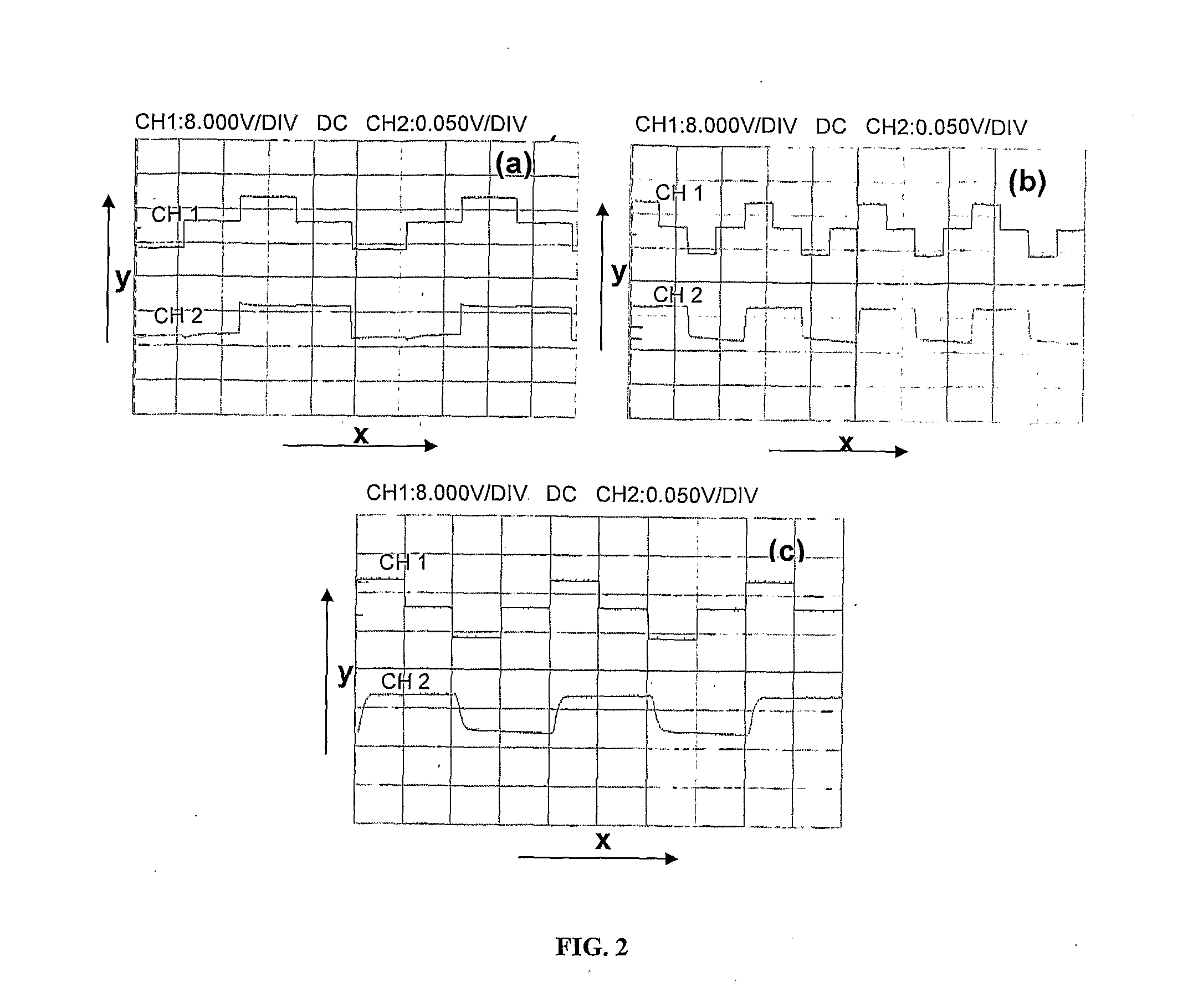

Image

  • Optical memory device based on dhlfc material and method of preparing the same
  • Optical memory device based on dhlfc material and method of preparing the same
  • Optical memory device based on dhlfc material and method of preparing the same

Examples


example 1

[0046]1 μl of glycerol is mixed with 2 mg of DHFLC material (FLC 6304, Rolic, Switzerland) (i.e glycerol is mixed with DHFLC in volume ratio of 0.5% of DHFLC) having a phase sequence of crystalline (−18° C.) smectic C* (60.5° C.) smectic A (64° C.) isotropic phase. The mixture is then filled at its isotropic temperature in the gap between the two substrates.

example 2

[0047]2 μl of glycerol is mixed with 3 mg of DHFLC material (LAHS 19, synthesis in Darmstadt, Germany) (i.e glycerol is mixed with DHFLC in the volume ratio of 6.6% of DHFLC) having the smectic C* phase at room temperature. The mixture is then filled at its isotropic temperature in the gap between the two substances.

example 3

[0048]1 μl of glycerol is mixed with 1 mg conventional DHFLC material (FLC 6304, Rolic, Switzerland) (i.e glycerol is mixed with DHFLC in the volume ratio of 10% of DHFLC) having a phase sequence of crystalline (−18° C.) smectic C* (60.5° C.) smectic A (64° C.) isotropic phase. The mixture is then filled at its isotropic temperature in the gap between the two substances.


PUM


Abstract

The invention relates to an optical memory device and method for the preparation of the optical memory device based on glycerol, a very common and versatile solvent, mixed deformed helix ferroelectric liquid crystal (DHFLC) having applications in ferroelectric liquid crystal based devices, the said method comprising the steps of forming patterns of different shapes and configurations by lithographic methods to obtain an effective electrode area of at least 4.5 mm on a glass substrate coated with indium tin oxide; depositing the patterned glass substrate with a polymer nylon 616 in the thickness range of 200 A-400 A; baking the coated substrate followed by hard rubbing of the polymer coated surface using buffing machine; photo lithographically developing spacer to maintain a uniform thickness of 3 μm; filling glycerol mixed deformed ferroelectric liquid crystal material in the space between the coated glass substrates, followed by sealing the sandwiched glass substrates at the periphery; heating and cooling the sandwiched glass substrates, followed by application of electric field across the sandwiched substrates for achieving the stable memory action and fastness of the response, by applying an AC and DC field across the device to obtain an optical memory device.

Description

FIELD OF THE INVENTION[0001]The present invention relates to an optical memory device and method for the preparation of the optical memory device. More particularly present invention based on deformed helix ferroelectric liquid crystal material mixed with solvent glycerol to be consequently used for manufacturing memory devices. The present invention relates to provide faster and long duration memory device having applications in electro-optical devices.BACKGROUND OF THE INVENTION[0002]Ferroelectric liquid crystals are generally known as being liquid crystals that exhibit smectic phases. These liquid crystals are used in image-producing displays by utilizing the properties that it possesses spontaneous polarization and that the direction of the spontaneous polarization changes under the influence of an external electric field.[0003]It is reported by N. A. Clark, and S. T. Lagerwall, Appl. Phys Lett, Vol. 36, 899 (1980), that liquid crystal electro-optical devices using ferroelectric...

Claims


Application Information

Patent Timeline
IPC IPC(8): G11C11/22B32B38/16B32B37/14B32B37/02
CPCG11C11/22C09K19/0225
Inventor JAI, PRAKASHKUMAR, AJAYCHOUDHARY, AMITMALIK, ANUCOONDOO, INDRANIBIRADAR, ASHOK MANIKRAO
Owner COUNCIL OF SCI & IND RES
Learn More