
Self aligned trench mosfet with integrated diode

a technology of trench mosfet and diode, which is applied in the direction of diodes, semiconductor devices, electrical apparatus, etc., can solve the problems of process control problems, complex fabrication techniques of trench mosfets, etc., and achieve the effect of fewer masks and small pitch

Active Publication Date: 2012-06-14
ALPHA & OMEGA SEMICON INC
View PDF36 Cites 84 Cited by
  • Summary
  • Abstract
  • Description
  • Claims
  • Application Information

AI Technical Summary

Benefits of technology

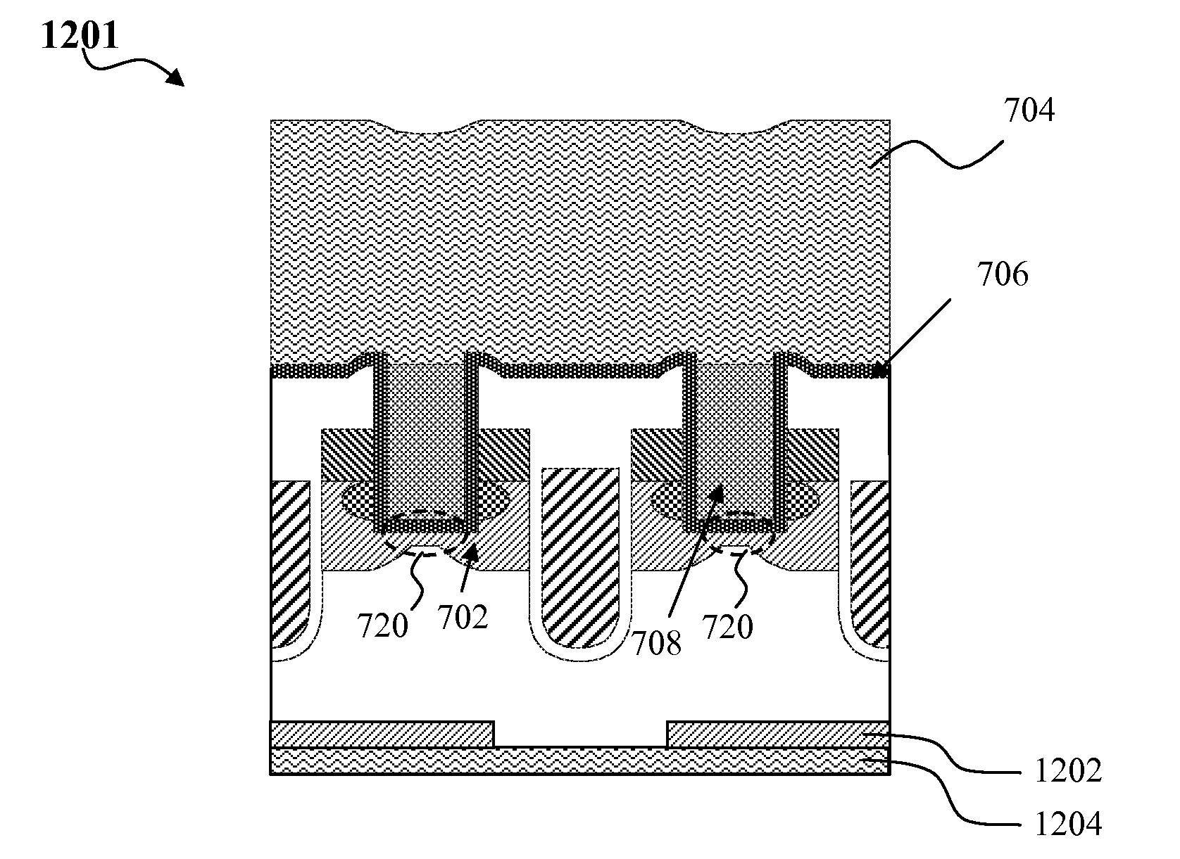
[0037]In FIG. 5J, the insulator 522 is etched back through a dry etch process where the oxide is etched down and stopped by endpoint below the top surface of the nitride layer 508. Nitride layer 508, poly layer 506 are etched away as shown in FIG. 5K. The remaining portions of the oxide layer 504 is also etched away with a light oxide etch to form a source / body contact. The light oxide etch is only performed for a short period of time to remove the thin oxide layer 504 while keeping the much thicker insulator layer 522 intact without needing a mask. Thus the nitride layer 508, poly layer 506, and oxide layer 504 serve as a sort of sacrificial structure.
[0096]Embodiments of the present invention provide for self-aligned fabrication of transistor devices such as MOSFET devices where source, body, and contact trenches are all self-aligned. This allows fabrication of devices with a smaller pitch than previous processes with fewer masks and without misalignment issues.

Problems solved by technology

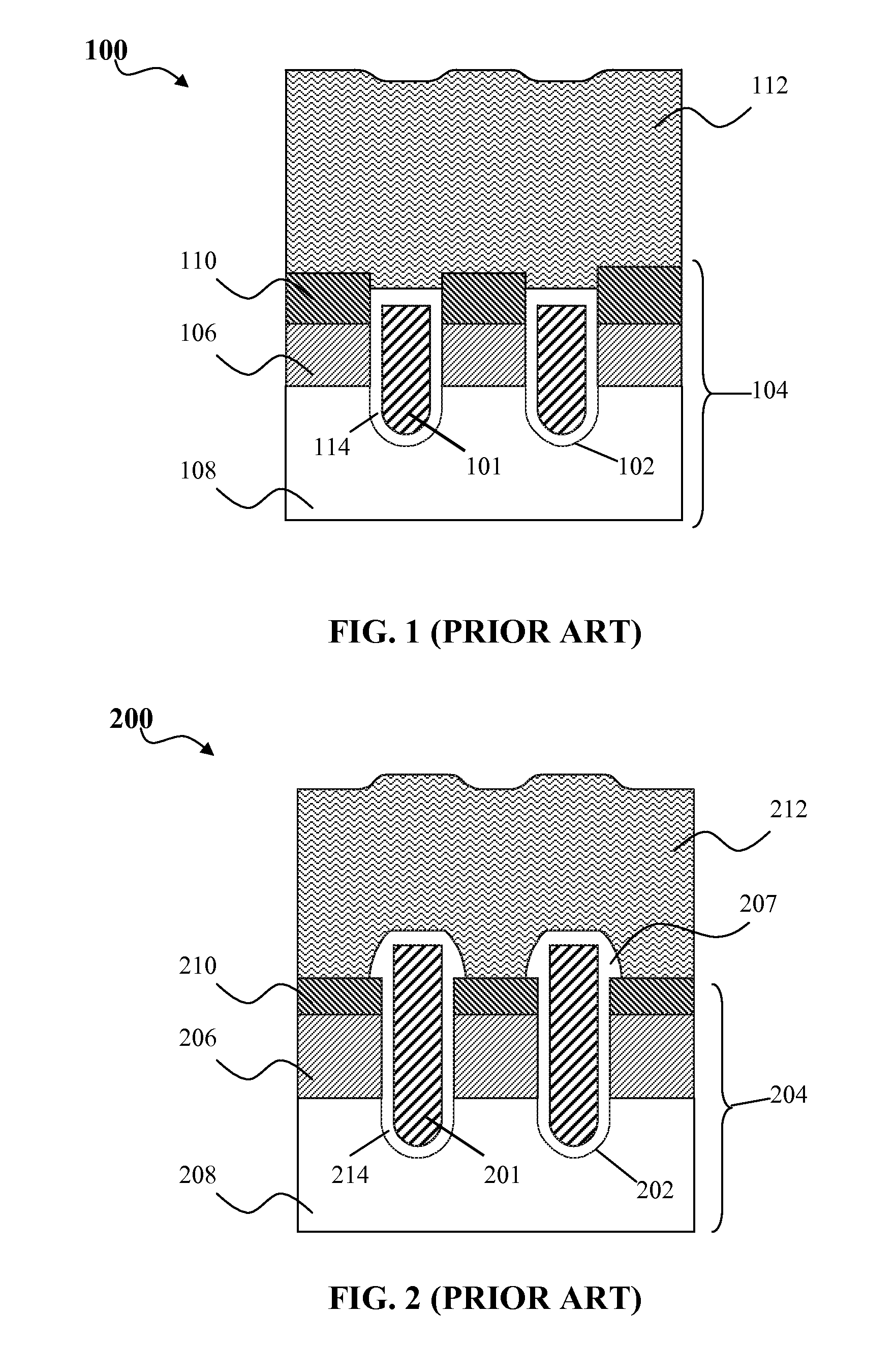
Existing fabrication techniques for trench MOSFETs are typically complex and expensive, usually requiring 6 or more masks to be applied during processing.
However, this raises process control issues, such as controlling the thickness and integrity of the thin oxide between the top corner of the gate electrode 201 and the metal 212.

Method used


Image

  • Self aligned trench mosfet with integrated diode
  • Self aligned trench mosfet with integrated diode
  • Self aligned trench mosfet with integrated diode

Examples


Embodiment Construction

[0026]Although the following detailed description contains many specific details for the purposes of illustration, anyone of ordinary skill in the art will appreciate that many variations and alterations to the following details are within the scope of the invention. Accordingly, the exemplary embodiments of the invention described below are set forth without any loss of generality to, and without imposing limitations upon, the claimed invention.

[0027]Embodiments of the present invention include methods of fabricating a self aligned trench transistors (e.g., trench MOSFETs) with an integrated Schottky diode using very few photoresist masks.

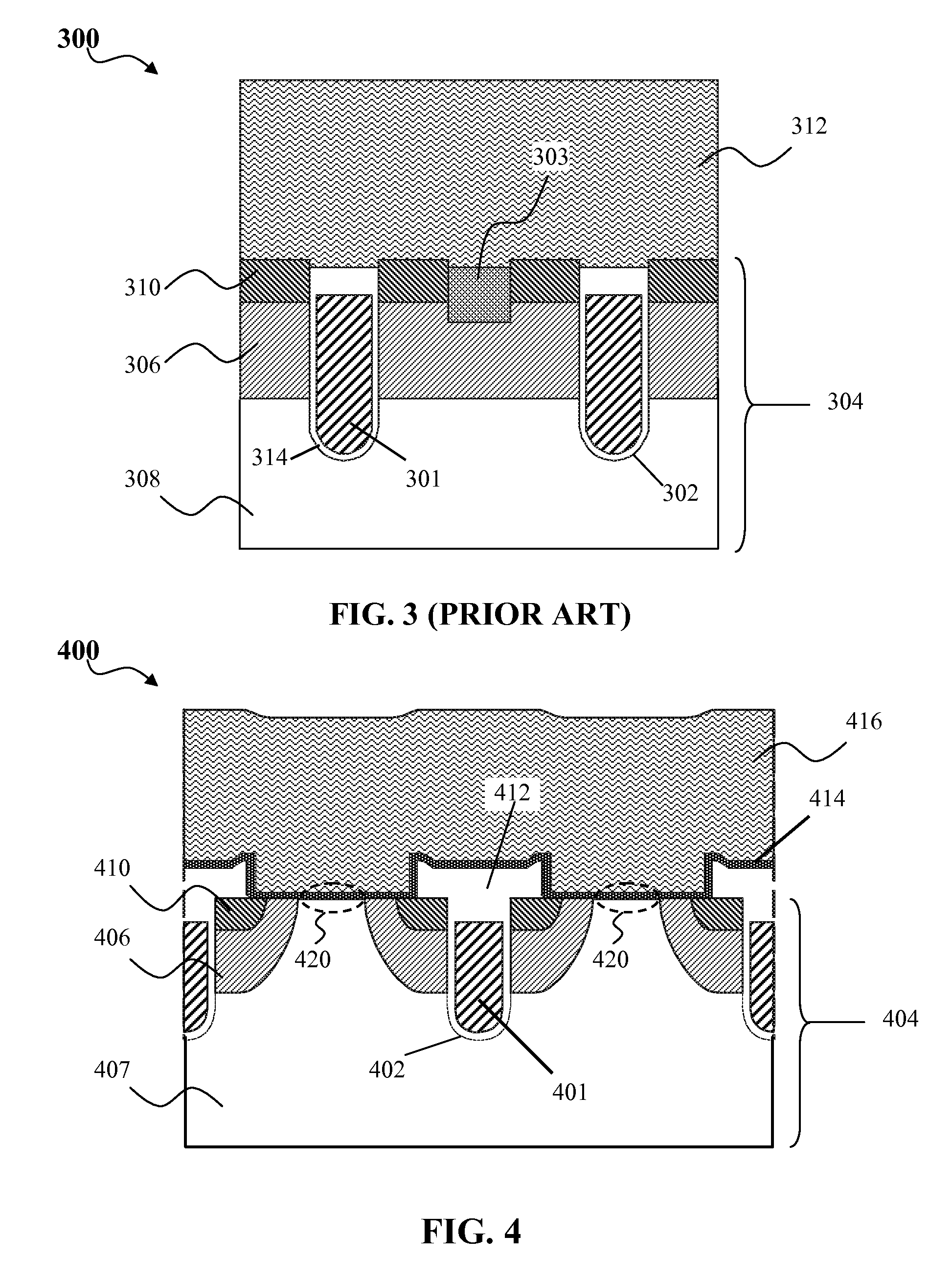
[0028]FIG. 4 is a diagram illustrating a top view of self aligned trench MOSFET device 400 with an integrated Schottky diode according to an embodiment of the present invention. As shown in FIG. 4, gate trenches 402 are formed in the semiconductor wafer 404 containing a semiconductor substrate which may include an epitaxial (epi) layer 407 formed ...


PUM


Abstract

Transistor devices can be fabricated with an integrated diode using a self-alignment. The device includes a doped semiconductor substrate having one or more electrically insulated gate electrodes formed in trenches in the substrate. One or more body regions are formed in a top portion of the substrate proximate each gate trench. One or more source regions are formed in a self-aligned fashion in a top portion of the body regions proximate each gate trench. One or more thick insulator portions are formed over the gate electrodes on a top surface of the substrate with spaces between adjacent thick insulator portions. A metal is formed on top of the substrate over the thick insulator portions. The metal forms a self-aligned contact to the substrate through the spaces between the thick insulator portions. An integrated diode is formed under the self-aligned contact.

Description

FIELD OF THE INVENTION[0001]This invention generally relates to trench MOSFET devices and more particularly to the methods for fabricating self aligned trench MOSFET devices with integrated Schottky diode.BACKGROUND OF THE INVENTION[0002]Many electronic circuit designs today have strict requirements on device performance parameters such as switching performance and on-state resistance. Trench power Metal Oxide Semiconductor Field Effect Transistors (MOSFET) devices are often used in such circuits. Existing fabrication techniques for trench MOSFETs are typically complex and expensive, usually requiring 6 or more masks to be applied during processing.[0003]FIG. 1 is a cross-sectional view of the conventional trench MOSFET device 100. As shown in FIG. 1, trenches 102 are formed in the semiconductor wafer 104 that includes a silicon substrate. By way of example, the silicon substrate may include an epitaxial (epi) layer 108 formed on a heavily doped bottom substrate layer (not shown). B...

Claims


Application Information

Patent Timeline
Patent Type & Authority Applications(United States)
IPC IPC(8): H01L29/739H01L21/28H01L21/331H10B12/00
CPCH01L29/1095H01L29/66704H01L29/41766H01L29/4236H01L29/456H01L29/47H01L29/66348H01L29/66719H01L29/66727H01L29/66734H01L29/7397H01L29/7805H01L29/7806H01L29/7811H01L29/7813H01L29/872H01L29/66666H01L29/7395H01L21/76877H01L27/10876H01L27/10823H01L21/7688H01L29/407H01L29/0834H10B12/34H10B12/053H01L27/0635H01L29/7804H01L29/8613
Inventor LUI, SIKBHALLA, ANUP
Owner ALPHA & OMEGA SEMICON INC
Learn More