Luminescent element, its preparation method thereof and luminescene method

a technology of luminescent elements and luminescenes, which is applied in the manufacture of electrode systems, electric discharge tubes/lamps, and discharge tubes luminescnet screens, etc., can solve the problems of significantly limiting the application of field emission devices, especially illumination, and low luminous efficiency, and achieves high internal quantum efficiency of luminescent substrates, high spontaneous emission of luminescent substrates, and low efficiency problems of luminescent materials

Inactive Publication Date: 2012-06-14
OCEANS KING LIGHTING SCI&TECH CO LTD
View PDF6 Cites 7 Cited by
  • Summary
  • Abstract
  • Description
  • Claims
  • Application Information

AI Technical Summary

Benefits of technology

[0004]In one aspect of the present disclosure, a luminescent element with high luminescent homogeneity, high luminous efficiency, good stability, simple structure and a preparation method with simple processes and low cost are desired.
[0005]In another aspect of the present disclosure, a luminescence method of the luminescent element with simple operation, good reliability, and improving luminous efficiency is also desired.
[0014]In the luminescent element described above, the metal layer with the metal microstructure is formed on the surface of the luminescent substrate and irradiated by the cathode-ray, the surface plasmon is thus generated between the metal layer and the luminescent substrate. Due to the surface plasmon effect, the internal quantum efficiency of the luminescent substrate is highly increased, and the spontaneous emission of the luminescent substrate is highly increased, so that the luminous efficiency of the luminescent substrate is improved and the low efficiency problem of the luminescent materials is overcomed. Accordingly, in the luminescence method of the luminescent element, once emitting cathode-ray to the metal layer, the surface plasmon will be formed between the metal layer and the luminescent substrate, thus the luminous efficiency and reliability are improved. The luminescent element has a simple two-layers structure including the luminescent substrate and the metal layer. In addition, there is a uniform interface formed between the luminescent substrate and the metal layer, so that an excellent luminescent homogeneity and stability are achieved. In the luminescence method of the luminescent element, once emitting cathode-ray to the metal layer, the surface plasmon will be formed between the metal layer and the luminescent substrate, thus improving the luminous efficiency and reliability of the luminescent substrate.
[0015]In the embodiment of the preparation method of the luminescent element, the luminescent element can be obtained by forming a metal layer on the luminescent substrate and annealing the luminescent substrate and the metal layer, thus the preparation method is simple and low cost. The luminescent element has a wide production and application prospect.

Problems solved by technology

Furthermore, materials such as the phosphor, luminescent substrate, luminescent film can be served as luminescent materials in field emission device, however, they all suffer from serious problems of low luminous efficiency, which significantly limit the application of the field emission device, especially in the application of illumination.

Method used


Image

  • Luminescent element, its preparation method thereof and luminescene method
  • Luminescent element, its preparation method thereof and luminescene method
  • Luminescent element, its preparation method thereof and luminescene method

Examples


example 1

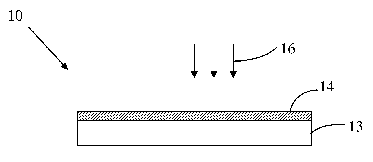
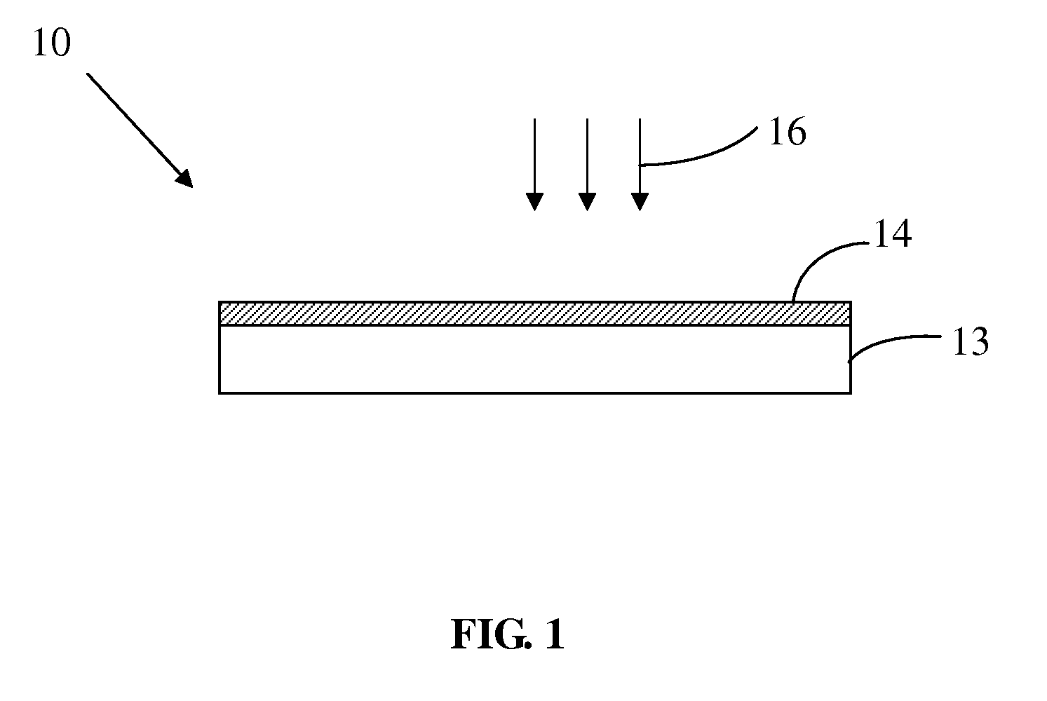
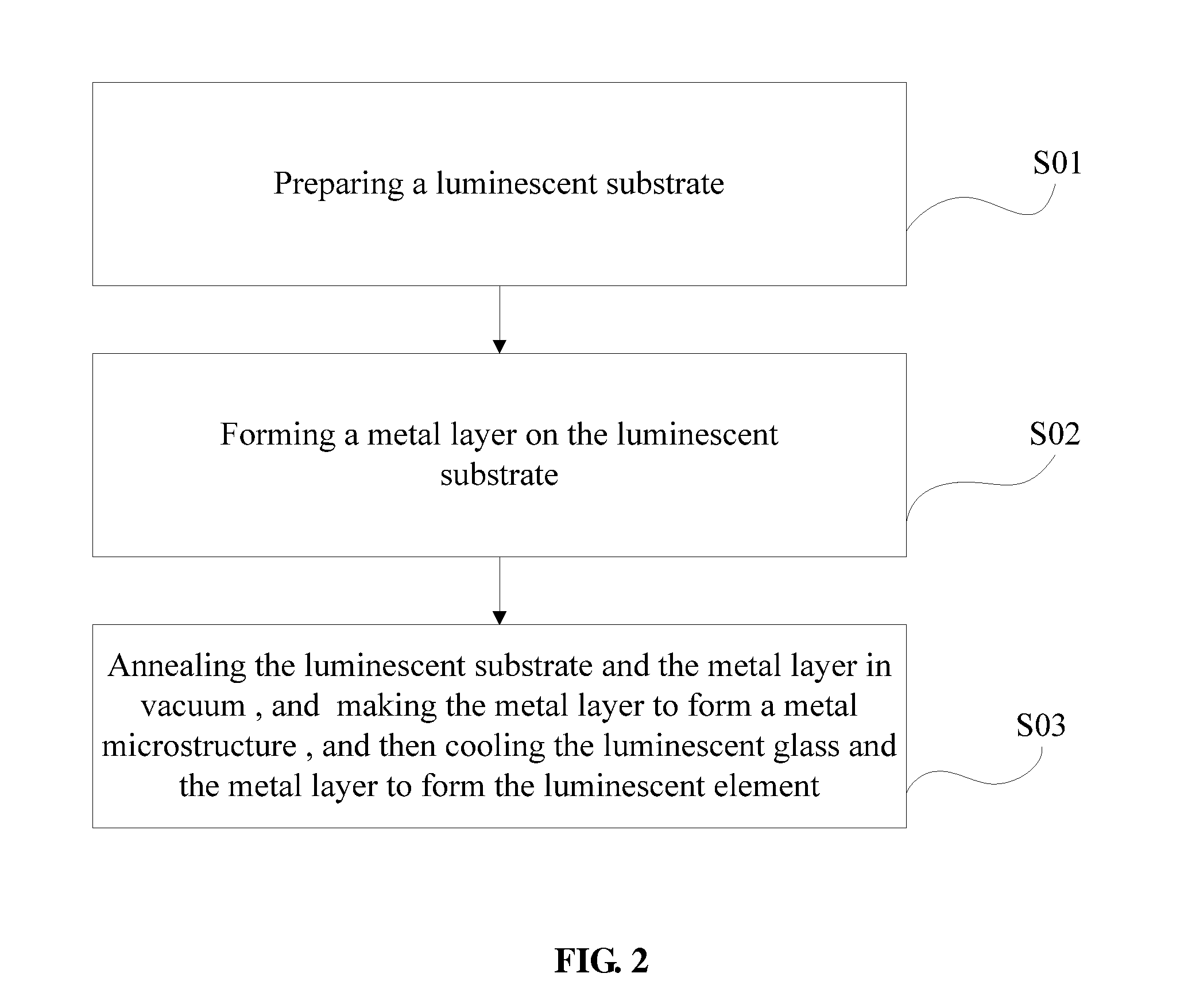
[0042]A phosphor with chemical composition Y2O3:Eu and a glass powder (the chemical composition of the glass powder are 20Na2O-20BaO-30B2O3-30SiO2) are mixed according to the mass proportion of 1:4 and then melted to prepare a luminescent glass doped with a luminescent material Y2O3:Eu. A Ag layer is deposited on a surface of the luminescent glass with thickness of 2 nm using a magnetron sputtering equipment, and then the Ag layer together with the luminescent glass are introduced in a vacuum environment with vacuum degree less than 1×10⁻³ Pa, annealed at 300° C. for 30 minutes and cooled to the room temperature to obtain a luminescent element of this embodiment.

[0043]A emission spectrum according to FIG. 4 is obtained when testing the emission spectrum of the luminescent element by bombarding the luminescent element using a cathode-ray generated by a electron gun which firstly penetrates the metal layer and then excites the luminescent glass doped with Y2O3:Eu to illuminate. The sp...

example 2

[0045]A phosphor with chemical composition Y2O3:Eu and a glass powder (the chemical composition of the glass powder are 20Na2O-20BaO-30B2O3-30SiO2) are mixed according to the mass proportion of 1:19 and then melted to prepare a luminescent glass doped with a luminescent material Y2O3:Eu. A Au layer is deposited on a surface of the luminescent glass with thickness of 0.5 nm using a magnetron sputtering equipment, and then the Au layer together with the luminescent glass are introduced in a vacuum environment with vacuum degree less than 1×10⁻³ Pa, annealed at 200° C. for 1 hour and cooled to the room temperature to obtain a luminescent element of this embodiment.

example 3

[0046]A phosphor with chemical composition Y2O3:Eu and a glass powder (the chemical composition of the glass powder are 20Na2O-20BaO-30B2O3-30SiO2) are mixed according to the mass proportion of 7:13 and then melted to prepare a luminescent glass doped with a luminescent material Y2O3:Eu. A Al layer is deposited on the surface of the luminescent glass with thickness of 200 nm using a magnetron sputtering equipment, and then the Al layer together with the luminescent glass are introduced in a vacuum environment with vacuum degree less than 1×10⁻³ Pa, annealed at 500° C. for 5 hours and cooled to the room temperature to obtain a luminescent element of this embodiment.


PUM

PropertyMeasurementUnit
thicknessaaaaaaaaaa
operating temperatureaaaaaaaaaa
thicknessaaaaaaaaaa

Abstract

A luminescent element includes a luminescent substrate; and a metal layer with a metal microstructure formed on a surface of the luminescent substrate; wherein the luminescent substrate has a luminescent material with a chemical composition: Y2O3:Eu. A preparation method of a luminescent element and a luminescence method are also provided. The luminescent element has good luminescence homogeneity, high luminescence efficiency, good luminescence stability and simple structure, and can be used in luminescent device with ultrahigh brightness.

Description

FIELD OF THE INVENTION[0001]The present disclosure relates to luminescent materials, and more particularly relates to a luminescent element including a glass substrate made of luminescent material, its preparation method thereof and luminescence method.BACKGROUND OF THE INVENTION[0002]The conventional materials used as luminescent substrate include phosphor, nanocrystal, glass and so on. Compared with the crystal and phosphor, the glass has advantages of transparent, rigid, excellent chemical stability and superior luminescent property. In addition, the glass can be easily manufactured into products with various shapes, such as display devices or light sources with various shapes and sizes.[0003]For example, in vacuum microelectronics, field emission devices usually use luminescent substrate as illuminant, which has shown a wide prospect in illumination and display techniques and draws a lot attention to domestic and foreign research institutes. The working principle of the field em...

Claims


Application Information

Patent Timeline
Patent Type & Authority Applications(United States)
IPC IPC(8): H01J29/88H05B33/10H05B33/14
CPCH05B33/14C03C3/068C03C4/12C03C17/09C03C2217/25H01J2329/20C09K11/7787H01J29/20H01J29/24H01J29/28C03C2218/15
Inventor ZHOU, MINGJIEMA, WENDOLIU, YUGANG
Owner OCEANS KING LIGHTING SCI&TECH CO LTD
Why Eureka
Try Eureka