Pattern Shape Estimation Method and Pattern Measuring Device

a pattern and shape technology, applied in the direction of instrumentation, semiconductor/solid-state device testing/measurement, program control, etc., can solve the problems of increasing the influence of process monitor measurement errors, and achieve stable and high-precision pattern shape selection and high precision

Inactive Publication Date: 2012-06-14
HITACHI HIGH-TECH CORP
View PDF6 Cites 56 Cited by
  • Summary
  • Abstract
  • Description
  • Claims
  • Application Information

AI Technical Summary

Benefits of technology

[0015]According to the illustrative embodiment above, by using results of the exposure process simulation, it is possible to employ a library including cross-sectional shapes similar to actual patterns; hence, it is possible to conduct stable and high-precision pattern shape selection, and the pattern shape estimation can be implemented with high precision.
[0016]Further, according to another illustrative embodiment described above, the exposure simulation can be appropriately evaluated.

Problems solved by technology

As the semiconductor pattern becomes finer, these measuring errors increasingly affect the process monitor.

Method used


Image

  • Pattern Shape Estimation Method and Pattern Measuring Device
  • Pattern Shape Estimation Method and Pattern Measuring Device
  • Pattern Shape Estimation Method and Pattern Measuring Device

Examples


embodiment 1

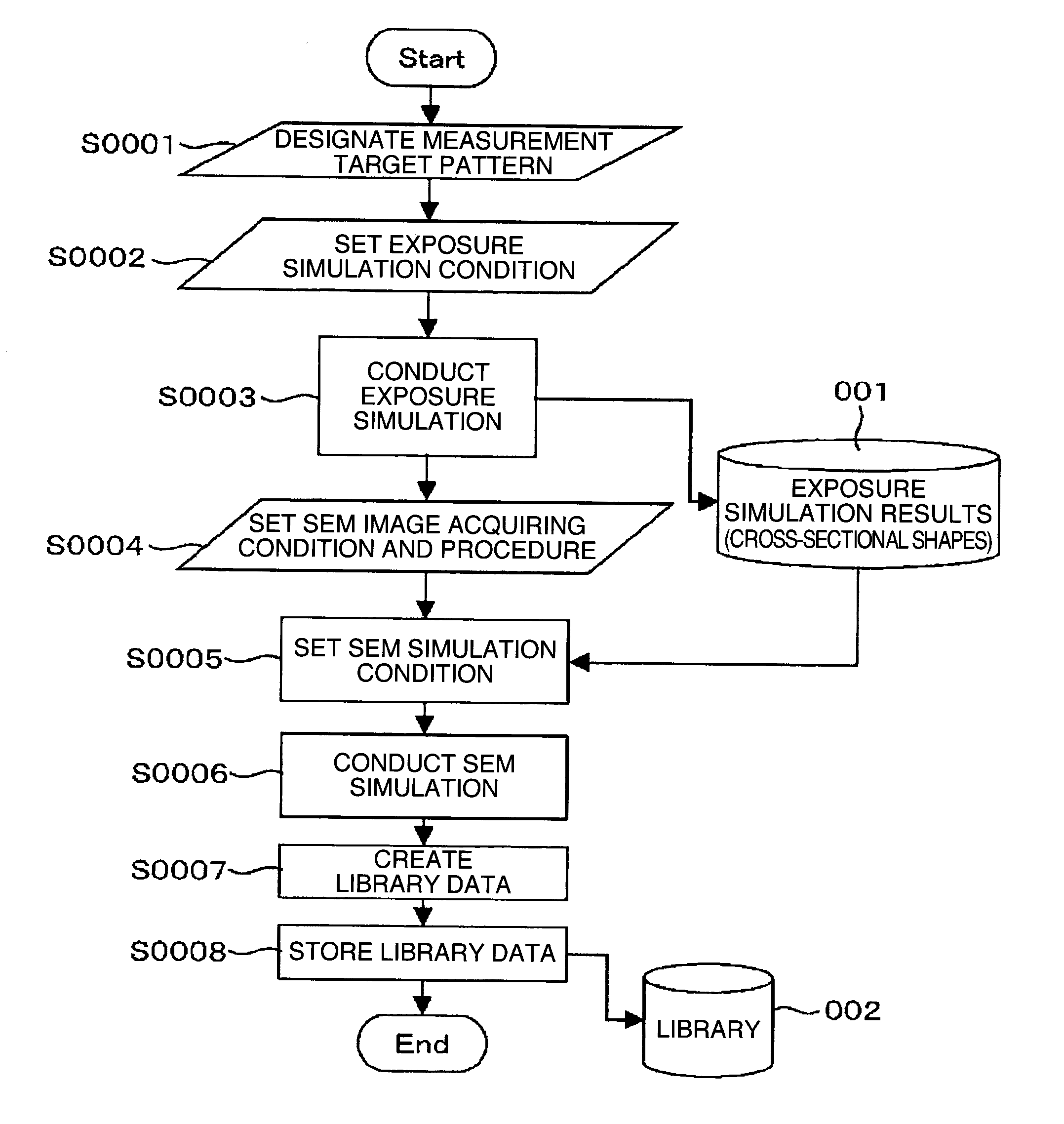
[0035]For the first embodiment, description will be given of a basic illustrative embodiment of a pattern dimension measuring method using exposure process simulation by referring to FIGS. 1 to 4.

[0036]FIG. 1 shows a procedure to create a simulation library and a procedure to create an image acquiring recipe (a file having recorded a procedure for automatic image acquisition as a device task list).

[0037]First, a measurement target pattern is designated (step S0001). The pattern may be designated while actually observing a pattern by an SEM or by use of pattern design data. Next, there is set a condition required to execute an exposure process simulation reflecting an exposure process to create a resist pattern as the designated measurement target (step S0002). Although details will be described later, it is necessary to set a mask, a light source, a rest parameter, and the like for the exposure simulation. The mask kind, the layout, the resist, and the kind of the underlay reflectio...

embodiment 2

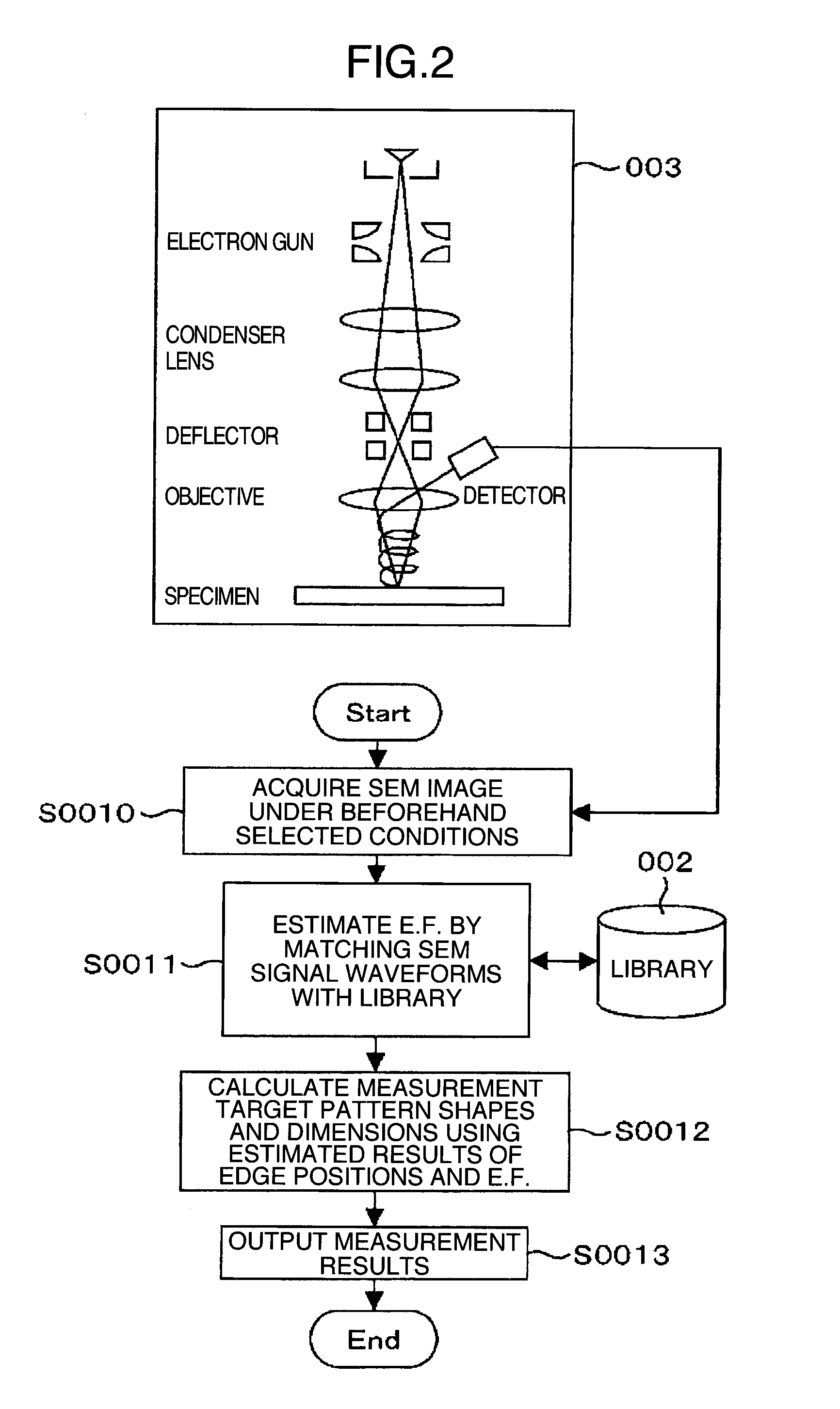
[0058]Next, description will be given of a method of evaluating the exposure simulation by use of the library matching method of the first embodiment. In the first embodiment, it is assumed that the exposure process simulation has been calibrated to match the actual sample in advance; however, actually, the calibration of the exposure process simulation itself also has many problems. Particularly, since there does not exist an effective unit to correctly measure the resist pattern cross-sectional shape at a high speed and at a low cost, the calibration of the exposure process simulation is difficult. In this regard, for the second embodiment, description will be given of a method of evaluating and adjusting the exposure process simulation by using the pattern shape measuring and dimension determining method through the library matching described in conjunction with the first embodiment.

[0059]For the first embodiment, description has been given of a situation to measure a pattern for...

embodiment 3

[0063]Next, description will be given of another method of evaluating an exposure simulation by using the library matching method of the first embodiment. For the second embodiment, description has been given of a situation in which although the exposure process simulation is not sufficiently adjusted, the cross-sectional shape set resultant from the exposure simulation conducted by changing the exposure energy and focus parameters fully expresses pattern shapes to be actually formed in the exposure process (the agreement degree of the library matching is sufficiently high). However, there exist many parameters associated with the exposure process; particularly, chemical characteristic parameters such as those of resist materials are not easily fitted through experiments. The exposure energy and focus differences and the like are relatively easily modeled; however, for the adjustment of the photosentitizer diffusion length and surface anti-solubility parameters which determine resis...


PUM


Abstract

The present invention aims at proposing a library creation method and a pattern shape estimation method in which it is possible, when estimating a shape based on comparison between an actual waveform and a library, to appropriately estimate the shape.
As an illustrative embodiment to achieve the object, there are proposed a method of selecting a pattern by referring to a library, a method of creating a library by use of pattern cross-sectional shapes calculated through an exposure process simulation in advance, and a method for selecting a pattern shape stored in the library.

Description

TECHNICAL FIELD[0001]The present invention relates to a method of and a device for measuring dimensions of a pattern formed on a specimen, and in particular, to a method of and a device for estimating a shape or measuring dimensions of a pattern formed through a lithography process.BACKGROUND ART[0002]In the semiconductor wafer production process, patterns to be formed in many layers on a wafer are rapidly becoming finer; hence, the process monitor to monitor whether or not these patterns are formed on the wafer according to designs is increasingly important. Particularly, wiring patterns including transistor gate wiring are deeply associated with their line widths and device operation characteristics; hence, the monitoring of the wiring production process is especially important.[0003]As a length measuring tool to measure the line width of fine wiring on the order of several tens of nanometers, there has been heretofore employed a scanning electron microscope (Critical dimension Sc...

Claims


Application Information

Patent Timeline
Patent Type & Authority Applications(United States)
IPC IPC(8): G06F17/50
CPCG01B15/04H01L22/12H01L2924/0002H01L2924/00
Inventor TANAKA, MAKIHASEGAWA, NORIOSHISHIDO, CHIEOSAKI, MAYUKA
Owner HITACHI HIGH-TECH CORP
Why Eureka
Try Eureka