Cobalt metal barrier layers

a technology of cobalt metal and barrier layer, which is applied in the direction of semiconductor devices, semiconductor/solid-state device details, electrical apparatus, etc., can solve the problems that the ever-smaller integrated circuit (ic) places enormous performance demands on the materials used to construct the ic devi

Inactive Publication Date: 2012-06-28
INTEL CORP
View PDF5 Cites 25 Cited by
  • Summary
  • Abstract
  • Description
  • Claims
  • Application Information

AI Technical Summary

Problems solved by technology

The desire for ever-smaller integrated circuits (IC) places enormous performance demands on the materials used to construct IC devices.

Method used


Image

  • Cobalt metal barrier layers
  • Cobalt metal barrier layers
  • Cobalt metal barrier layers

Examples


Embodiment Construction

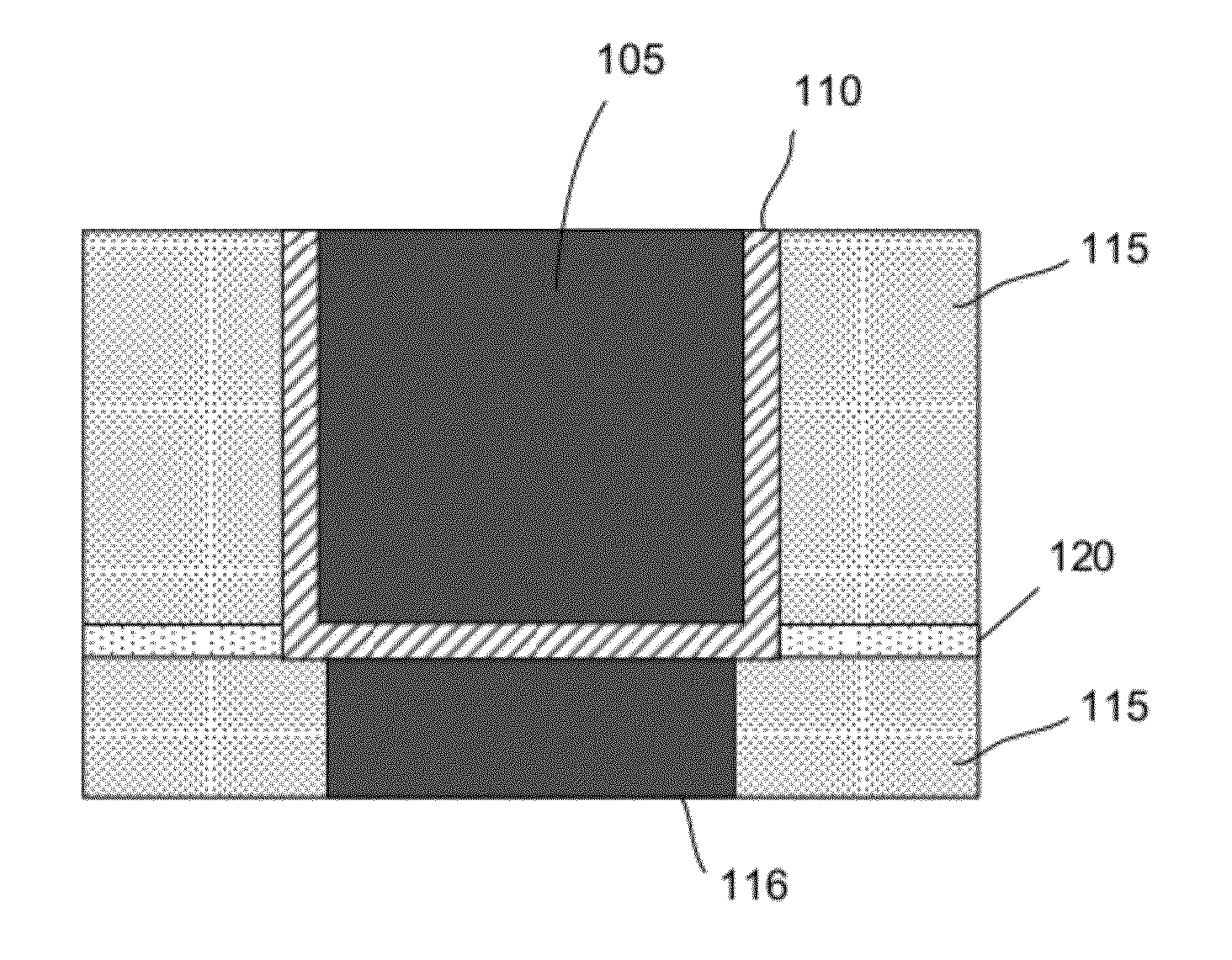
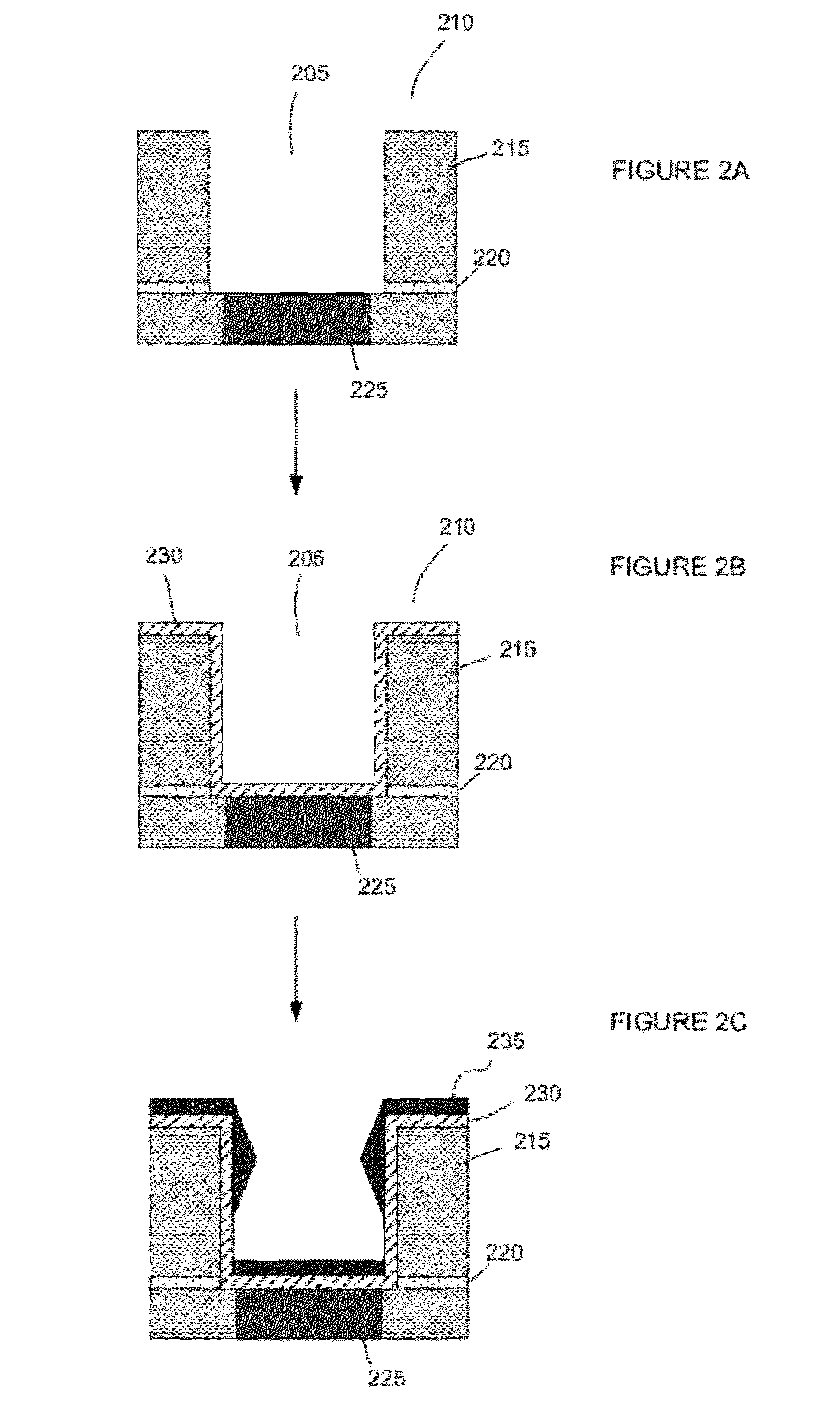
[0009]Electronic connections between the electronic devices (e.g., transistors) in an integrated circuit (IC) chip are currently typically created using copper metal or alloys of copper metal. Devices in an IC chip can be placed not only across the surface of the IC chip but devices can also be stacked in a plurality of layers on the IC chip. Electrical interconnections between electronic devices that make up the IC chip are built using vias and trenches that are filled with conducting material. Layer(s) of insulating materials, frequently, low-k dielectric materials, separate the various components and devices in the IC chip.

[0010]The substrate on which the devices of the IC circuit chip are built is, for example, a silicon wafer or a silicon-on-insulator substrate. Silicon wafers are substrates that are typically used in the semiconductor processing industry, although embodiments of the invention are not dependent on the type of substrate used. The substrate could also be comprise...


PUM

PropertyMeasurementUnit
thickaaaaaaaaaa
thickaaaaaaaaaa
diameteraaaaaaaaaa

Abstract

Electrical interconnects for integrated circuits and methods of fabrication of interconnects are provided. Devices are provided comprising copper interconnects having metal liner layers comprising cobalt and a metal selected from the group consisting of Ru, Pt, Ir, Pd, Re, or Rh. Devices having barrier layers comprising ruthenium and cobalt are provided. Methods include providing a substrate having a trench or via formed therein, forming a metal layer, the metal being selected from the group consisting of Ru, Pt, Ir, Pd, Re, and Rh, onto surfaces of the feature, depositing a copper seed layer comprising a cobalt dopant, and depositing copper into the feature.

Description

CROSS REFERENCE TO RELATED APPLICATIONS[0001]The present application is related to U.S. application Ser. No. 12 / 890,462, entitled “Barrier Layers,” filed Sep. 24, 2010.BACKGROUND OF THE INVENTION[0002]1. Field of the Invention[0003]The embodiments of the present invention relate generally to semiconductor processing, integrated circuits, barrier layers for metal interconnects, low-k dielectrics, and gapfill during deposition in semiconductor processing applications.[0004]2. Background Information[0005]The desire for ever-smaller integrated circuits (IC) places enormous performance demands on the materials used to construct IC devices. In general, an integrated circuit chip is also known as a microchip, a silicon chip, or a chip. IC chips are found in a variety of common devices, such as the microprocessors in computers, cars, televisions, CD players, and cellular phones. A plurality of IC chips are typically built on a silicon wafer (a thin silicon disk, having a diameter, for examp...

Claims


Application Information

Patent Timeline
Patent Type & Authority Applications(United States)
IPC IPC(8): H01L23/532H01L21/768
CPCH01L21/76843H01L21/76858H01L21/76867H01L21/76883H01L23/53238H01L2924/0002H01L2924/00
Inventor AKOLKAR, ROHAN N.CLARKE, JAMES S.
Owner INTEL CORP
Why Eureka
Try Eureka