Feature size reduction

a technology of feature size and reduction, applied in the direction of semiconductor/solid-state device manufacturing, basic electric elements, electric apparatus, etc., can solve the problems of ever-smaller integrated circuits (ic) placing enormous performance demands on techniques and materials

Active Publication Date: 2012-06-28
INTEL CORP
View PDF0 Cites 369 Cited by
  • Summary
  • Abstract
  • Description
  • Claims
  • Application Information

AI Technical Summary

Problems solved by technology

The push for ever-smaller integrated circuits (IC) places enormous performance demands on the techniques and materials used to construct IC devices.

Method used


Image

  • Feature size reduction
  • Feature size reduction
  • Feature size reduction

Examples


Embodiment Construction

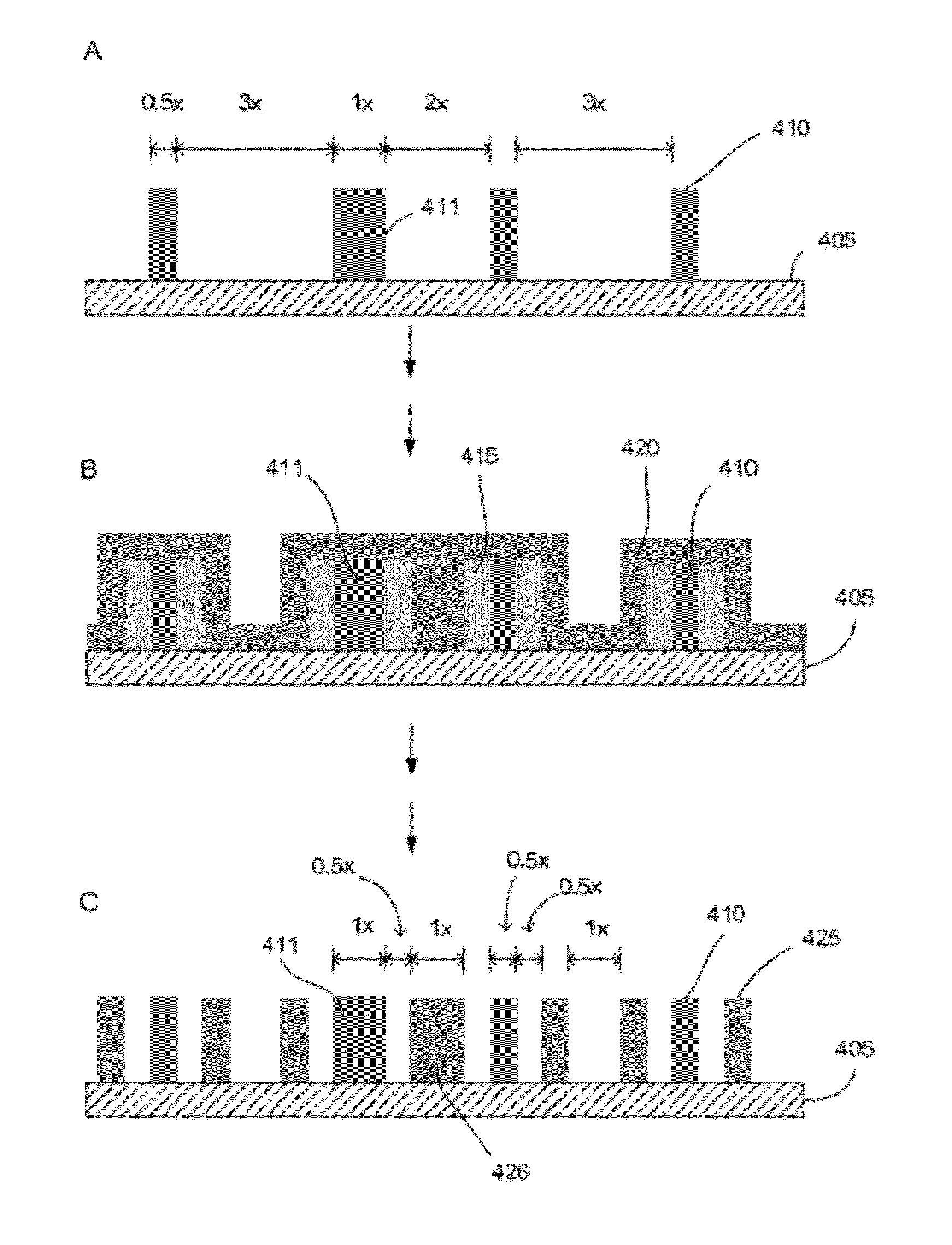
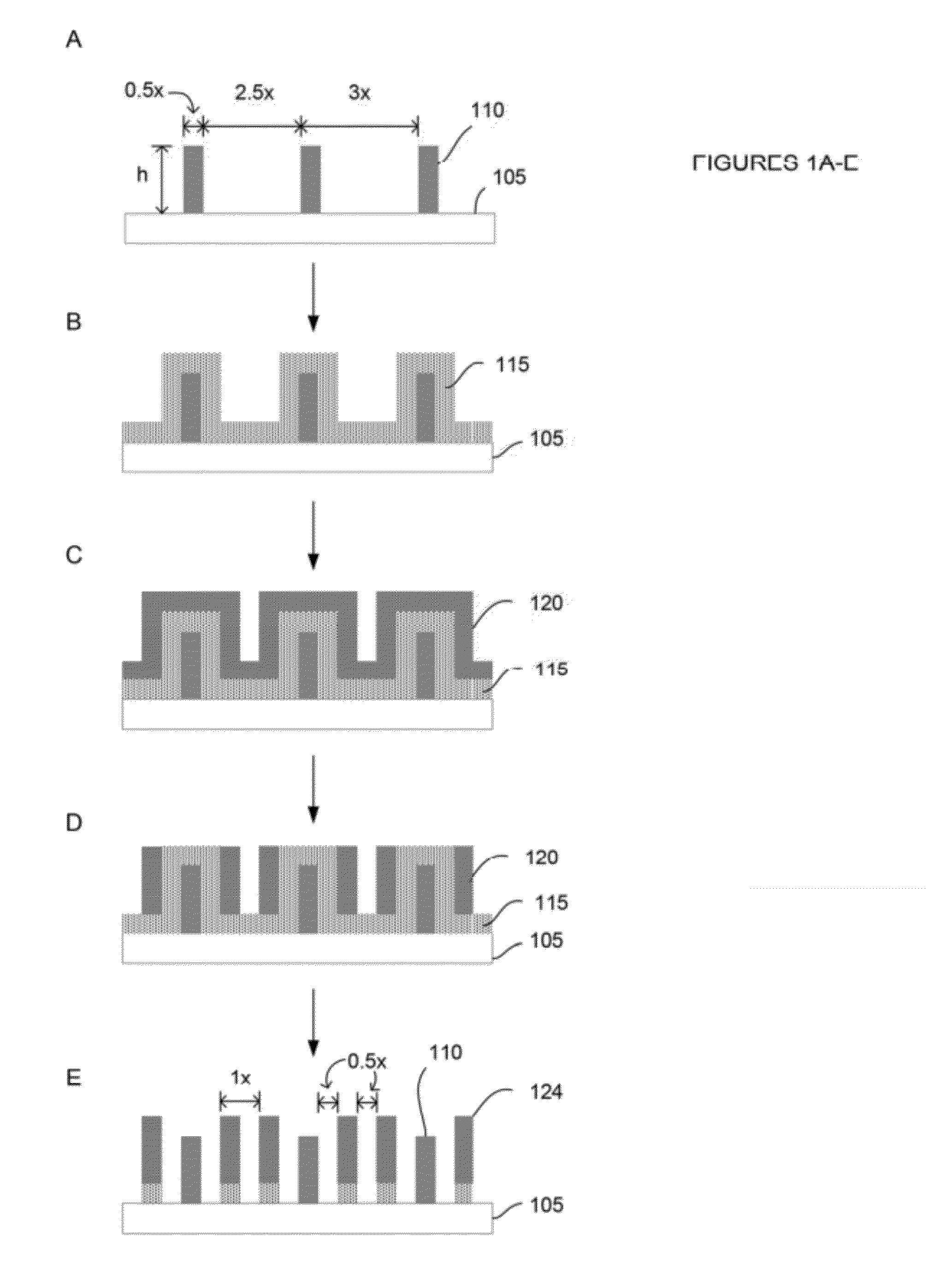
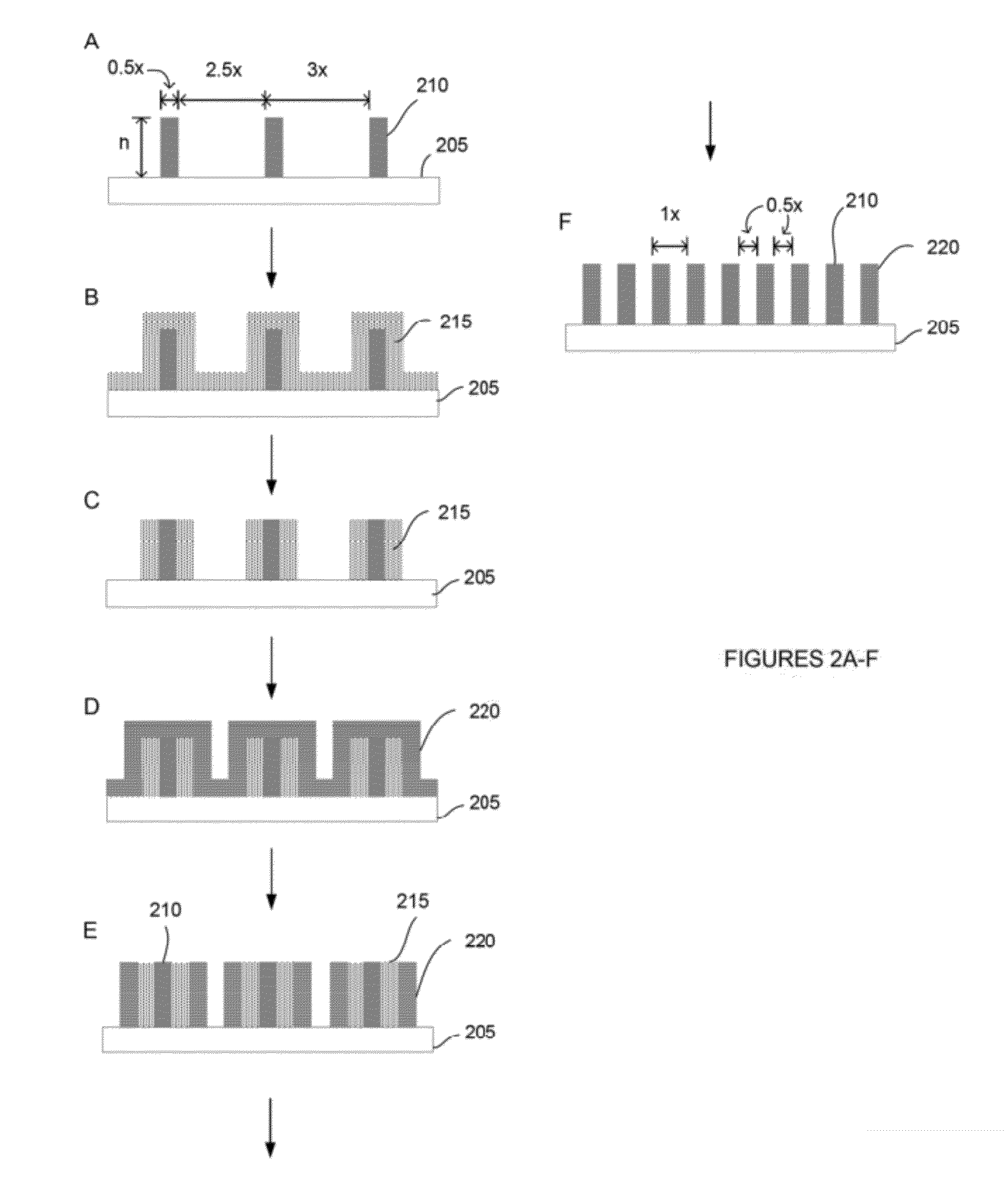
[0009]A variety of processes are used to fabricate the devices that make up an integrated circuit chip, such as, deposition processes that lay down materials, and lithographic and etching processes that remove materials in selected areas. The continued miniaturization of semiconductor chips requires the definition of features on the 45 nm scale and below. One common process used to create features is photo lithography (lithography). Lithography typically involves depositing a layer of photoresist on the wafer surface over the material to be patterned, patterning the photoresist with electromagnetic radiation (typically deep ultraviolet light), and removing the photoresist in patterned (or unpatterned, depending on the type of photoresist) areas. The layer beneath the photoresist that has been exposed is then etched in a typical process. Patterning the photoresist with electromagnetic radiation can be done for example, by exposing the photoresist through a mask. The pattern of the ma...


PUM


Abstract

Methods for semiconductor device fabrication are provided. Features are created using spacers. Methods include creating a pattern comprised of at least two first features on the substrate surface, depositing a first conformal layer on the at least two first features, depositing a second conformal layer on the first conformal layer, partially removing the second conformal layer to partially expose the first conformal layer, and partially removing the first conformal layer from between the first features and the second conformal layer thereby creating at least two second features. Optionally the first conformal film is partially etched back before the second conformal film is deposited.

Description

BACKGROUND OF THE INVENTION[0001]1. Field of the Invention[0002]The embodiments of the present invention relate generally to semiconductor processing and manufacture, integrated circuits, and spacers used to create devices in integrated circuits.[0003]2. Background Information[0004]The push for ever-smaller integrated circuits (IC) places enormous performance demands on the techniques and materials used to construct IC devices. In general, an integrated circuit chip is also known as a microchip, a silicon chip, or a chip. IC chips are found in a variety of common devices, such as the microprocessors in computers, cars, televisions, CD players, and cellular phones. A plurality of IC chips are typically built on a silicon wafer (a thin silicon disk, having a diameter, for example, of 300 mm) and after processing the wafer is diced apart to create individual chips. A 1 cm2 IC chip having feature sizes around of about 65 nm can comprise hundreds of millions of components. Current techno...

Claims


Application Information

Patent Timeline
Patent Type & Authority Applications(United States)
IPC IPC(8): H01L21/31
CPCH01L21/0338H01L21/0337
Inventor TAN, ELLIOT N.HARPER, MICHAEL K.
Owner INTEL CORP
Why Eureka
Try Eureka