Nitride semiconductor device and method of producing the same

a technology of nitride semiconductor and semiconductor device, which is applied in the direction of semiconductor/solid-state device manufacturing, semiconductor devices, electrical apparatus, etc., can solve the problems of insufficient light output power of nitride semiconductor device and inability to obtain sufficient current characteristics with hemts, etc., to achieve excellent current characteristics, good flatness and crystallinity, good flatness

Active Publication Date: 2012-07-12
DOWA ELECTRONICS MATERIALS CO LTD
View PDF2 Cites 42 Cited by
  • Summary
  • Abstract
  • Description
  • Claims
  • Application Information

AI Technical Summary

Benefits of technology

[0026]The present invention can provide a nitride semiconductor device excellent in current characteristics, in which a superlattice strain buffer layer using AlGaN layers having a low Al content or GaN layers is formed with good flatness on an AlN strain buffer layer on a substrate, and a nitride semiconductor layer with good flatness and crystallinity is formed on the superlattice strain buffer layer.
[0027]Further, the present invention can provide a nitride semiconductor device having high light output power, in which a superlattice strain buffer layer using AlGaN layers having a low Al content or GaN layers is formed with good flatness on an AlN strain buffer layer on a substrate, and an n-type nitride semiconductor layer with good flatness and crystallinity is formed on the superlattice strain buffer layer.

Problems solved by technology

However, the light output power of the above ultraviolet LEDs (nitride semiconductor devices) has not been sufficient.
However, with respect to the above-described HEMTs, the flatness of the surface of the channel layer (i-type AlGaN layer) fowled on the buffer layer made of GaN is not sufficient; thus, sufficient current characteristics cannot been obtained with the HEMTs.

Method used


Image

  • Nitride semiconductor device and method of producing the same
  • Nitride semiconductor device and method of producing the same
  • Nitride semiconductor device and method of producing the same

Examples


example 1

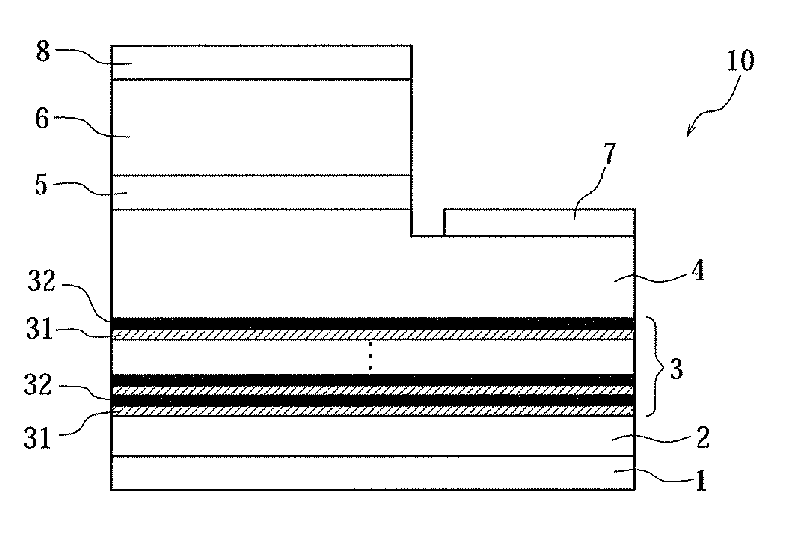
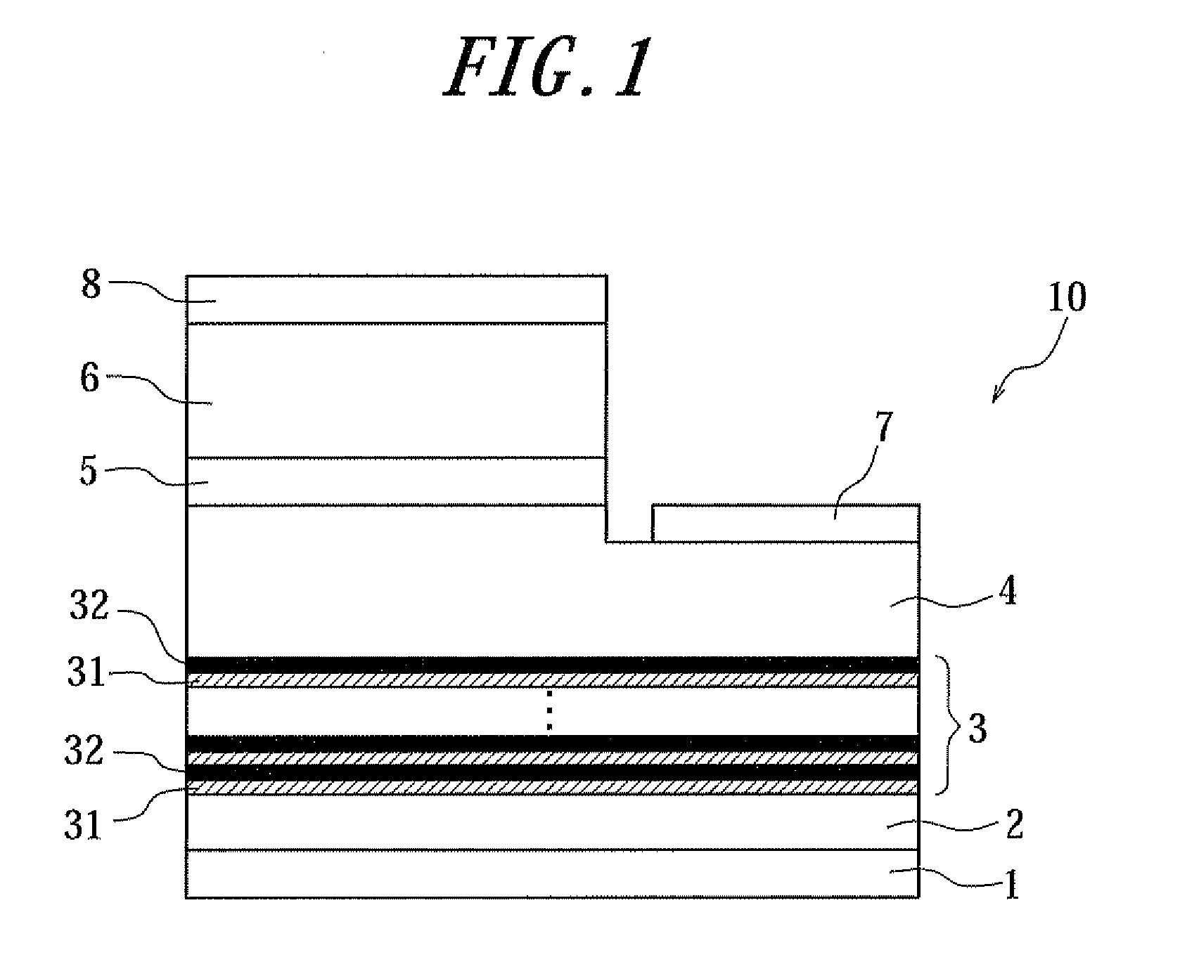
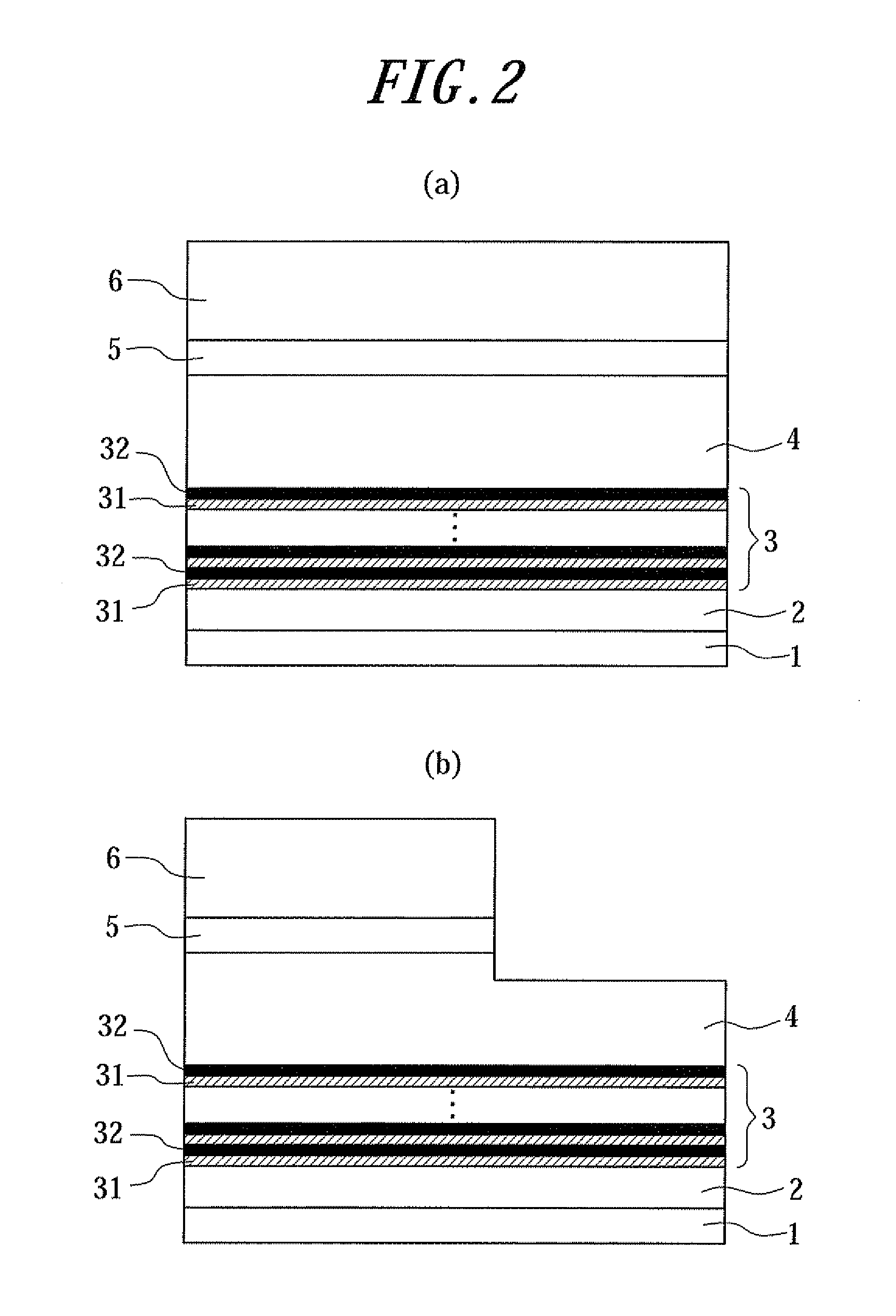
[0058]An AlN layer (thickness: 27 nm) was formed as an initial layer by MOCVD on an AlN template having an AlN strain buffer layer on the (0001) plane of a sapphire substrate, and then a superlattice strain buffer layer, an n-type nitride semiconductor layer, a light emitting layer, and a p-type nitride semiconductor layer were epitaxially grown thereon sequentially to form an epitaxial laminate. After that, the n-type nitride semiconductor layer was partially exposed by dry etching. An n-side electrode (Ti / Al) was formed on the n-type nitride semiconductor layer, and a p-side electrode (Ni / Au) was formed on the p-type nitride semiconductor layer to manufacture a nitride semiconductor device. Note that the thickness of the AlN strain buffer layer used was 800 nm, and its dislocation density was 1×1010 cm−2 or less. Note that the superlattice strain buffer layer had a structure in which first layers were made of GaN and a superlattice layer I having 20 sets of alternately stacked AlN...

example 2-1

[0061]A nitride semiconductor device was manufactured in a similar manner to Example 1 except for that first layers in a superlattice strain buffer layer were made of AlxGa1−xN (x=0.15) instead of GaN.

example 2-2

[0063]A nitride semiconductor device was manufactured in a similar manner to Example 1 except for that first layers in a superlattice strain buffer layer were made of AlxGa1−xN (x=0.23) instead of GaN.


PUM

PropertyMeasurementUnit
thicknessaaaaaaaaaa
emission wavelengthaaaaaaaaaa
thicknessaaaaaaaaaa

Abstract

A nitride semiconductor device is provided, in which a superlattice strain buffer layer using AlGaN layers having a low Al content or GaN layers is formed with good flatness, and a nitride semiconductor layer with good flatness and crystallinity is formed on the superlattice strain buffer layer. A nitride semiconductor device includes a substrate; an AlN strain buffer layer made of AlN formed on the substrate; a superlattice strain buffer layer formed on the AlN strain buffer layer; and a nitride semiconductor layer formed on the superlattice strain buffer layer, and is characterized in that the superlattice strain buffer layer has a superlattice structure formed by alternately stacking first layers made of AlxGa1−xN (0≦x≦0.25), which further contain p-type impurity, and second layers made of AlN.

Description

TECHNICAL FIELD[0001]The present invention relates to a nitride semiconductor device and a method of producing the nitride semiconductor device.RELATED ART[0002]In recent years, ultraviolet LEDs (light emitting diodes) which emit light in an ultraviolet region, particularly of which emission wavelength is less than 365 nm, have attracted attention as LEDs that can be favorably used in the fields of sterilization, water purification, medical treatment, illumination, high-density optical recording, and the like. Further, in recent years, electronic devices such as HEMTs using compound semiconductors are also attracting attention.[0003]Devices having a device structure formed using an AlGaN-based thin film as a device material are known as such ultraviolet LEDs. Further, with respect to ultraviolet LEDs having a device structure formed using such an AlGaN-based thin film, various approaches have been made to improve light output power of the ultraviolet LEDs by obtaining high quality A...

Claims


Application Information

Patent Timeline
Patent Type & Authority Applications(United States)
IPC IPC(8): H01L33/06H01L21/20H01L33/32H01L29/15
CPCH01L33/007H01L33/32H01L33/12H01L33/04
Inventor OOSHIKA, YOSHIKAZUMATSUURA, TETSUYA
Owner DOWA ELECTRONICS MATERIALS CO LTD
Why Eureka
Try Eureka