Plasma processing apparatus and wave retardation plate used therein
- Summary
- Abstract
- Description
- Claims
- Application Information
AI Technical Summary
Benefits of technology
Problems solved by technology
Method used
Image
Examples
first embodiment
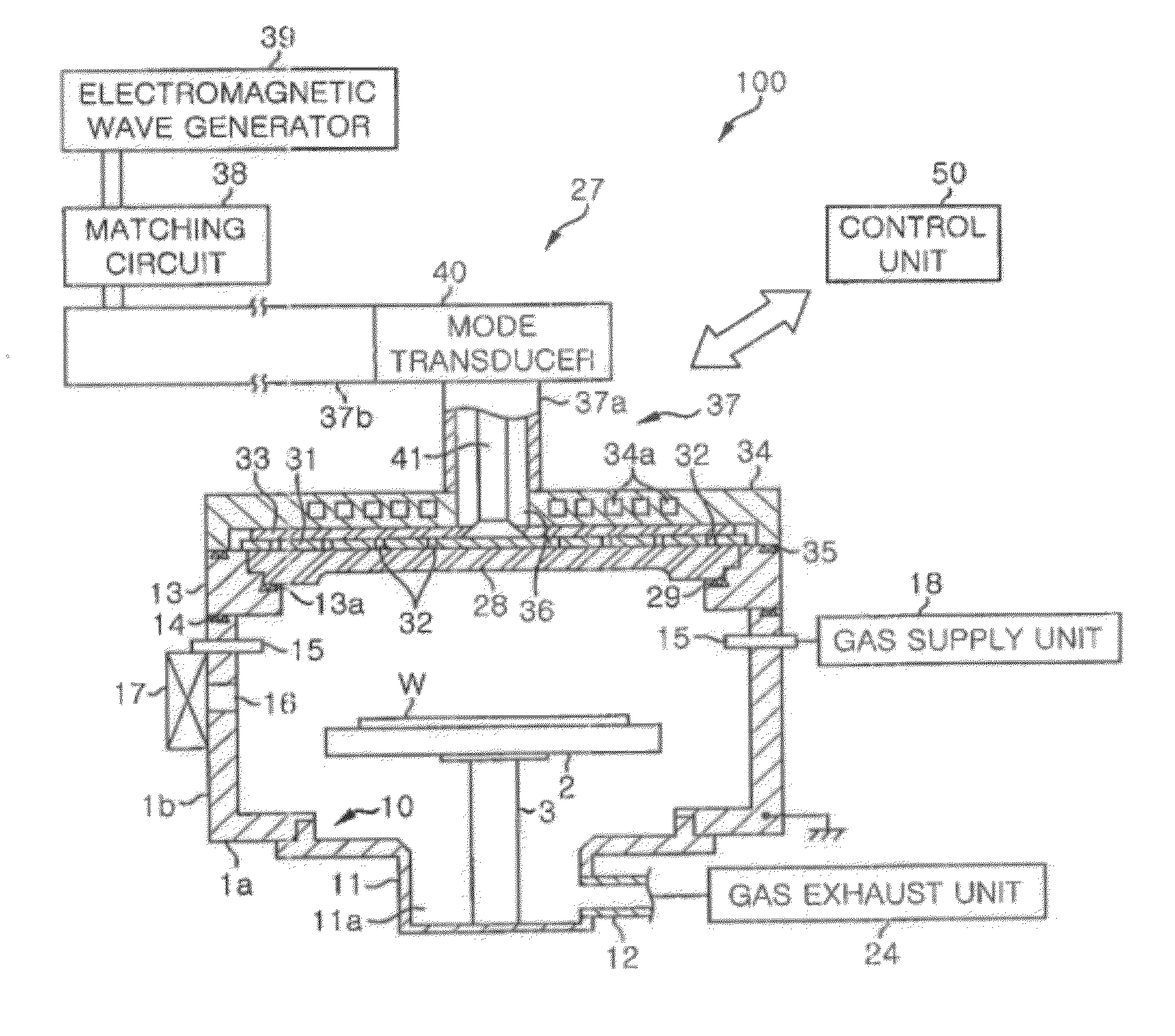
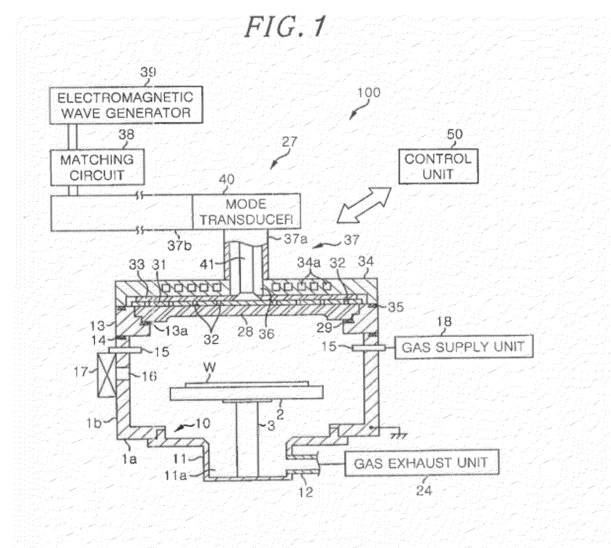
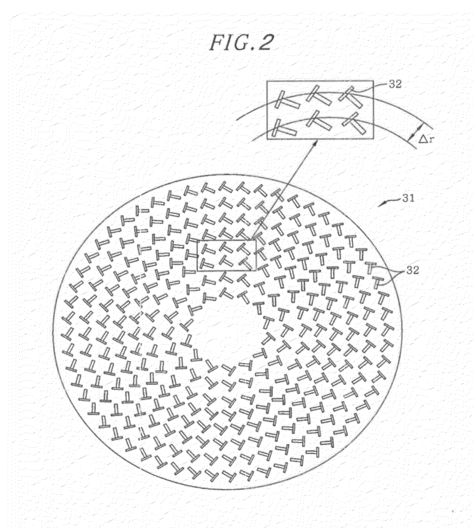
[0031]Hereinafter, embodiments of the present invention will be described in detail with reference to the accompanying drawings. FIG. 1 is a cross sectional view schematically showing a configuration example of a plasma processing apparatus 100 in accordance with a first embodiment of the present invention. FIG. 2 is a top view showing a planar antenna used in the plasma processing apparatus 100 shown in FIG. 1. The plasma processing apparatus 100 is configured as a plasma processing apparatus capable of generating a plasma of a high density and a low electron temperature by introducing a microwave into the processing chamber by using a planar antenna having a plurality of slots, particularly an RLSA (Radial Line Slot Antenna). The plasma processing apparatus 100 can perform a process using a plasma having a density of about 109 / cm3 to 1013 / cm3 and a low electron temperature of about 2 eV or less. Accordingly, the plasma processing apparatus 100 can be preferably used in a manufactu...
second embodiment
[0075]Hereinafter, a plasma processing apparatus in accordance with a second embodiment of the plasma processing apparatus of the present invention will be described with reference to FIGS. 11 to 13. The plasma processing apparatus of the present embodiment is the same as the plasma processing apparatus 100 (FIG. 1) of the first embodiment except for the configuration of the wave retardation plate 33. Therefore, the redundant description will be omitted, and only the configuration of the wave retardation plate 33 will be described. FIG. 11 is a top view of the wave retardation plate 33 of the second embodiment. The wave retardation plate 33 includes a small-diameter member 101 disposed at an inner side, a large-diameter member 103 surrounding the small-diameter member 101, and a plurality of (eight in FIG. 11) pieces 107 provided between the small-diameter member 101 and the large-diameter member 103. All the pieces 107 are made of a dielectric material. The pieces 107 may be made o...
third embodiment
[0084]Hereinafter, a plasma processing apparatus in accordance with a third embodiment of the present invention will be described with reference to FIGS. 14 to 16. The plasma processing apparatus of the present embodiment is the same as the plasma processing apparatus 100 (FIG. 1) of the first embodiment except for the configuration of the wave retardation plate 33. Therefore, the redundant description will be omitted, and only the configuration of the wave retardation plate 33 will be described. FIG. 14 is a perspective view showing an exterior configuration of the wave retardation plate 33 used in the third embodiment. FIG. 15 is a cross sectional view of principal parts of the plasma processing apparatus and shows the attachment state of the wave retardation plate 33. The wave retardation plate 33 includes a disc-shaped member 115 having substantially the same area as that of the planar antenna plate 31 and a ring-shaped member 117 provided on the disc-shaped member 115 in an ove...
PUM
| Property | Measurement | Unit |
|---|---|---|
| Thickness | aaaaa | aaaaa |
| Wavelength | aaaaa | aaaaa |
| Permittivity | aaaaa | aaaaa |
Abstract
Description
Claims
Application Information


