Layout method for soft-error hard electronics, and radiation hardened logic cell

a logic cell and hard electronics technology, applied in the field of soft-error hard electronics and radiation-hardened logic cells, can solve problems such as voltage pulses in circuits, and achieve the effect of reducing the effect of single event and protecting against soft errors

Active Publication Date: 2012-07-19
LILJA KLAS OLOF
View PDF7 Cites 5 Cited by
  • Summary
  • Abstract
  • Description
  • Claims
  • Application Information

AI Technical Summary

Benefits of technology

[0014]This invention comprises a unique new layout method, which takes advantage of the overall circuit response to a single event effect, and, furthermore, comprises circuit cells, with layout, which are protected against soft errors. The method uses an arrangement of critical contact areas in such a way that single event pulses in the circuit, that are generated on multiple nodes, act to oppose each other and hence cancel (or greatly reduce the effect of the single event). In the case that a primary and secondary circuit is used to maintain, or process the signal in a circuit, addition rules, described in section 4, are used, so that no possibility remains that a error is generated in both primary and secondary circuit, and hence that the combination of primary and secondary circuit will be fully error free.

Problems solved by technology

This leads to current pulses on the circuit nets, connected to these contact areas, which, in their turn, cause voltage pulses in the circuit which can upset a sequential element (latch, flip-flop) or propagate through combinational logic and be latched in as errors at the next sequential element in the circuit.

Method used


Image

  • Layout method for soft-error hard electronics, and radiation hardened logic cell
  • Layout method for soft-error hard electronics, and radiation hardened logic cell
  • Layout method for soft-error hard electronics, and radiation hardened logic cell

Examples


Embodiment Construction

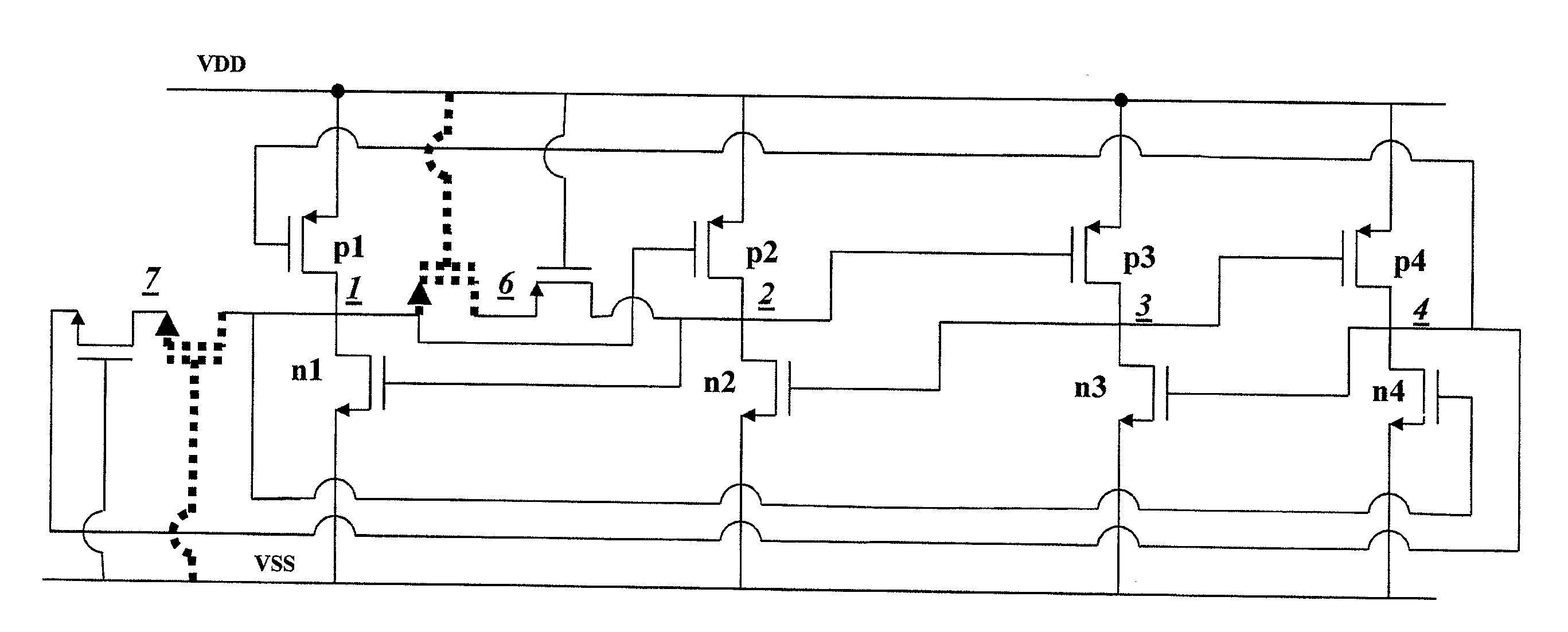
[0028]This invention comprises a unique new layout method, which takes advantage of the overall circuit response to a single event effect. It also includes specific circuit cells with layout, which have been constructed in accordance with the new layout method.

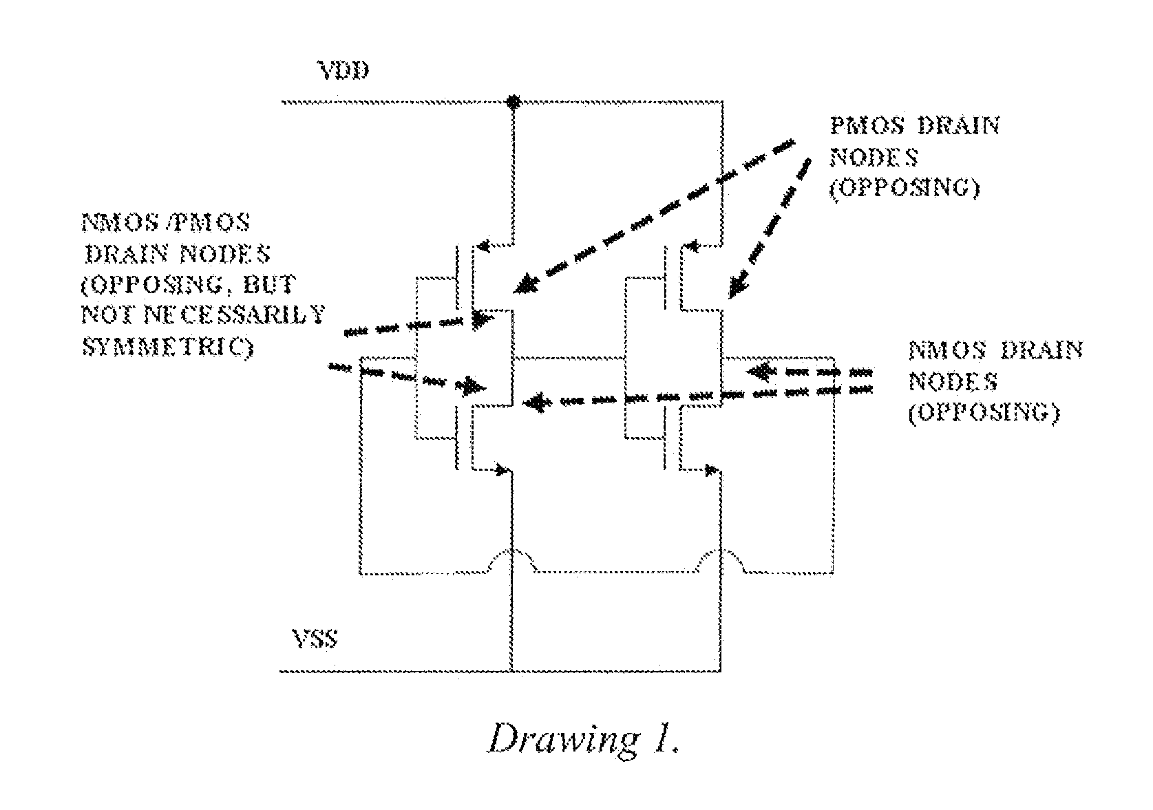
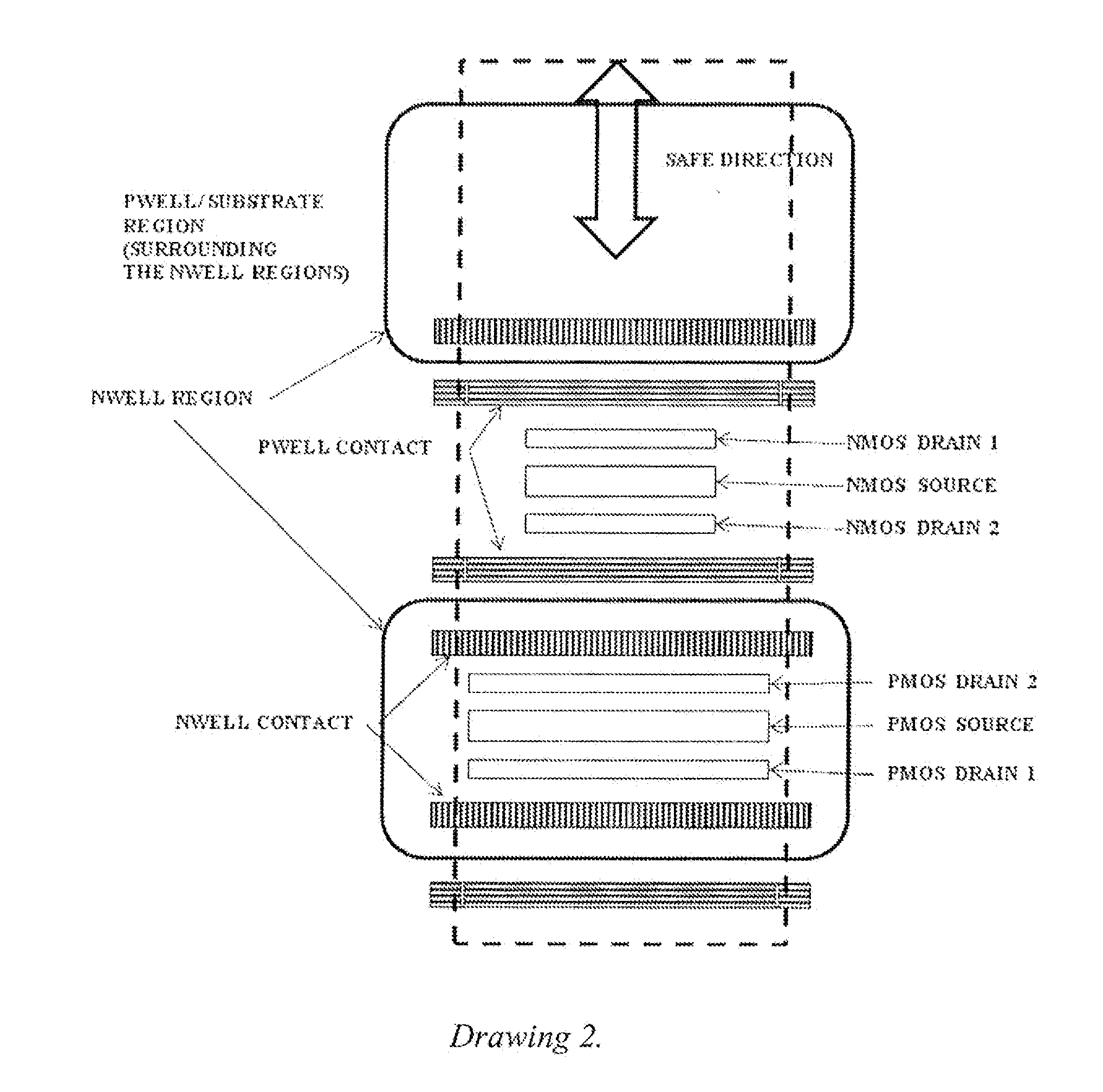
[0029]A radiation generated single event (soft-) error (SEE) occurs when the charge, generated in the semiconductor material by one or more (e.g. secondary) charged particles, is collected by contact areas. The contact areas are the low resistivity regions on, or in, the semiconductor substrate, which are connected to a net in the circuit, e.g., the source and drain areas in a MOSFET technology. A circuit net (or node) refers to a part of the circuit, connected by low resistivity regions (metal), which maintains a certain voltage value (referred to as the voltage state of the net) throughout its' extent. A net can be connected to any number of contact areas.

[0030]The charge collected by contact areas during a single event, lea...


PUM


Abstract

This invention comprises a layout method to effectively protect logic circuits against soft errors (non-destructive errors) and circuit cells, with layout, which are protected against soft errors. In particular, the method protects against cases where multiple nodes in circuit are affected by a single event. These events lead to multiple errors in the circuit, and while several methods exist to deal with single node errors, multiple node errors are very hard to deal with using any currently existing protection methods. The method is particularly useful for CMOS based logic circuits in modern technologies (.ltoreq.90 nm), where the occurrence of multiple node pulses becomes high (due to the high integration level). It uses a unique layout configuration, which makes the circuits protected against single event generated soft-errors.

Description

CROSS REFERENCE TO RELATED APPLICATIONS[0001]This application is a divisional application, claiming the priority of co-pending U.S. application Ser. No. 12 / 354,655, Entitled: “Layout Method for Soft-Error Hard Electronics, and Radiation Hardened Logic Cell”, filed Jan. 15, 2009, also claiming priority to U.S. application No. 61 / 011,599, Entitled: “Layout Methodology for Soft-Error Hard Electronics”, filed Jan. 17, 2008, also claiming priority to U.S. provisional application No. 61 / 011,989, Entitled: “Robust Cell Layout Synthesis Methodology for Soft-Error Hard Electronics”, filed Jan. 22, 2008, also claiming priority to U.S. provisional application No. 61 / 068,483, Entitled: “Circuit and Layout for a Radiation Hard Sequential Circuit Element”, filed Mar. 7, 2008, also claiming priority to U.S. provisional application No. 61 / 123,003, Entitled: “Design Technique, and Layout and Circuit Configurations, for Radiation Hardening of Logic Circuits”, filed Apr. 5, 2008, which are incorporate...

Claims


Application Information

Patent Timeline
Patent Type & Authority Applications(United States)
IPC IPC(8): G06F17/50
CPCG06F17/5068G06F2217/12G06F17/5022H03K19/00338H03K19/20H03K19/0033G06F2119/18G06F30/39Y02P90/02H03K19/0175H03K19/173G06F30/33G06F30/392
Inventor LILJA, KLAS OLOF
Owner LILJA KLAS OLOF
Why Eureka
Try Eureka