Substrate for flexible device, thin film transistor substrate for flexible device, flexible device, substrate for thin film element, thin film element, thin film transistor, method for manufacturing substrate for thin film element, method for manufacturing thin film element, and method for manufacturing thin film transistor

a flexible device and substrate technology, applied in the direction of synthetic resin layered products, coatings, chemistry apparatus and processes, etc., can solve the problems of surface irregularities, deterioration of surface irregularities, etc., to prevent the occurrence of detachment or cracking of tft, improve the wettability of a polyimide resin composition to a metal base material, and improve the electrical performance of tft

Active Publication Date: 2012-07-26
DAI NIPPON PRINTING CO LTD
View PDF5 Cites 61 Cited by
  • Summary
  • Abstract
  • Description
  • Claims
  • Application Information

AI Technical Summary

Benefits of technology

[0093]According to the present invention, since a planarizing layer is formed on a metal foil, the surface irregularities of the metal foil surface can be planarized. Therefore, deterioration of the electrical performance of a TFT can be prevented, and also, since a contact adhesive layer is formed, the adhesiveness between the substrate for a flexible device and the TFT is satisfactory, and there is obtained an effect that the occurrence of detachment or cracking in the TFT can be prevented.
[0094]Furthermore, according to the present invention, since the wettability of a polyimide resin composition to a metal base material can be improved by subjecting the metal base material to a chemical treatment, when the polyimide resin composition is applied on the metal base material, the polyimide resin composition can be uniformly applied. A...

Problems solved by technology

Even in the case where the metal foil is an electrolytic foil, surface irregularities exist on the surface.
Therefore, there is a problem that when a TFT is produced on a flexible substrate, the electrical performance of the TFT is deteriorated.
Also, in the case of the method of using a polyimide film, since polyimide films usually contain particles for the purpose of enhancing anti-blocking properties, surface irregularities exist on the surface.
Thus, similarly, there is a problem that when a TFT is produced on a flexible substrate, the electrical performance of the TFT is deteriorated.
However, even if a polyimide layer having satisfactory surface smoothness has been obtained, since polyimide has relatively high hygroscopic properties, there is a problem that in a process of producing a TFT on a flexible substrate, the TFT undergoes cracking or detachment as the dimension of the polyimide layer changes due to moisture.
Furthermore, the dimension of the polyimide layer changes not only because of moisture but also because of heat, similarly, there occurs a problem of cracking or detachment of the TFT.
Generally, since polyimides lack solubility in solvents and are difficult to process, in many cases, a desired shape is produced while the compound is in the form of a precursor, and then the precursor is converted to polyimide by being subjected to heating.
Many of polyimide precursors are unstable to heat or water, and the precursors tend to have poor storage stability, such as requiring refrigerated storage.
However, when these polyimides are used, the polymers tend to deteriorate in the film properties such as heat resistance, chemical resistance, the coefficient of linear thermal expansion, and the coefficient of hygroscopic expansion, as compared with systems using polyimide precursors.
In this case, when the polyimide resin composition is applied, if the wettability to the base material is poor, it is difficult to uniformly apply the resin composition on the base material, so that there occurs a problem in the flatness of the surface after film formation.
Also, if the effect is conspicuous, there is a problem that repelling or foaming may occur, pinholes may be formed in the film, or the like.
Therefore, there is a problem that the characteri...

Method used


Image

  • Substrate for flexible device, thin film transistor substrate for flexible device, flexible device, substrate for thin film element, thin film element, thin film transistor, method for manufacturing substrate for thin film element, method for manufacturing thin film element, and method for manufacturing thin film transistor
  • Substrate for flexible device, thin film transistor substrate for flexible device, flexible device, substrate for thin film element, thin film element, thin film transistor, method for manufacturing substrate for thin film element, method for manufacturing thin film element, and method for manufacturing thin film transistor
  • Substrate for flexible device, thin film transistor substrate for flexible device, flexible device, substrate for thin film element, thin film element, thin film transistor, method for manufacturing substrate for thin film element, method for manufacturing thin film element, and method for manufacturing thin film transistor

Examples


first embodiment

(I) First Embodiment

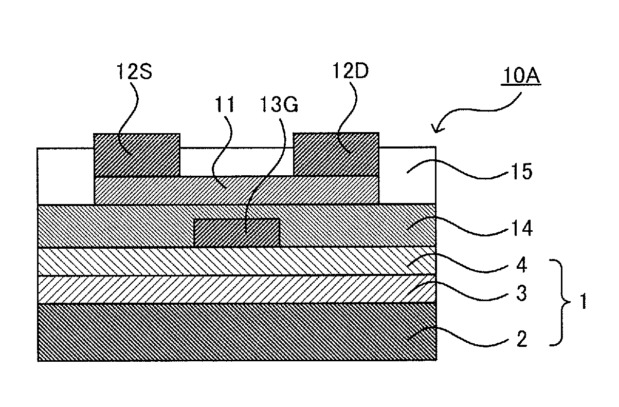
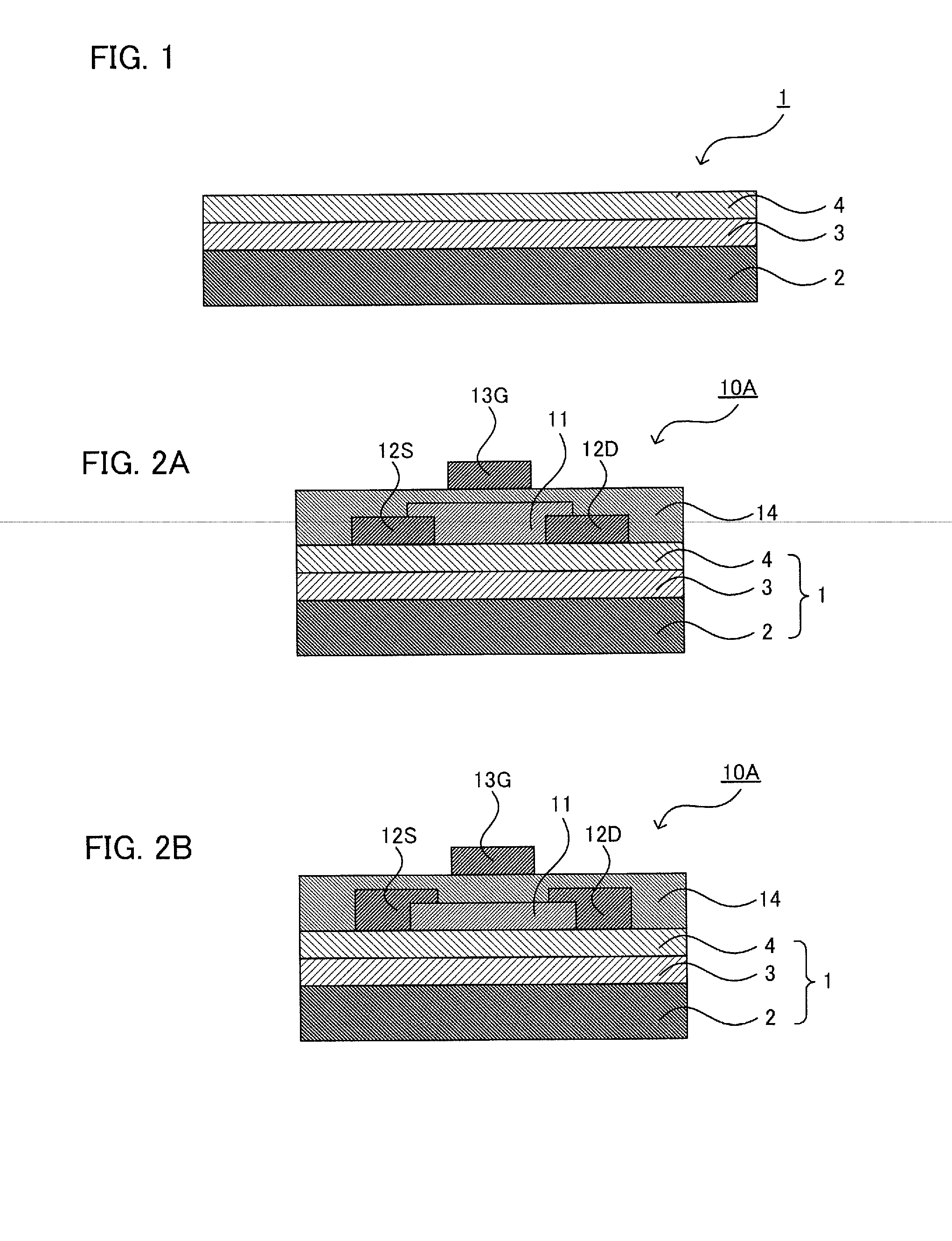
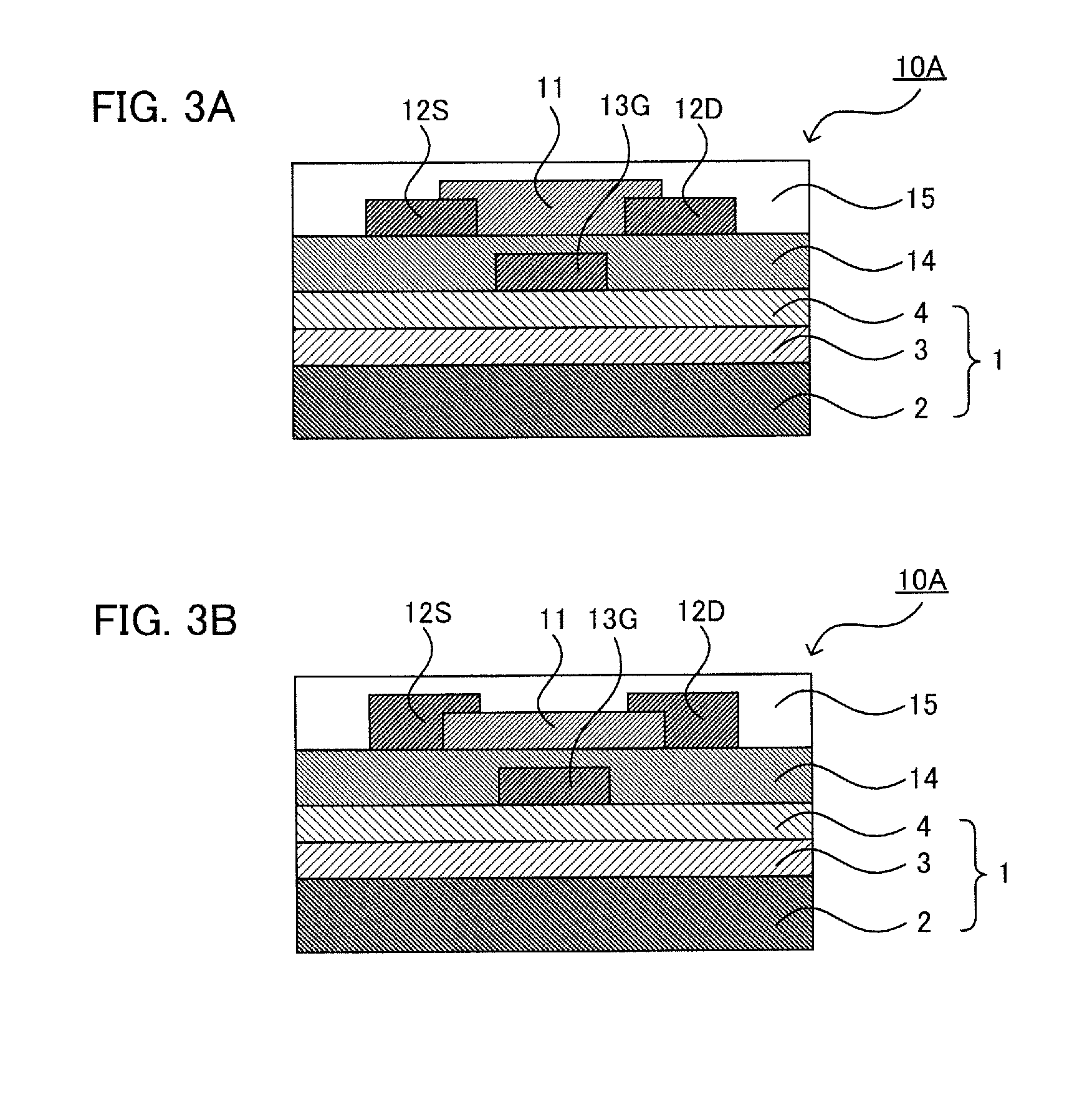
[0353]The first embodiment of the method for manufacturing a substrate for a thin film element of the present invention comprises steps of: a metal base material surface treatment step of subjecting a metal base material to a chemical treatment, and an insulating layer forming step of applying a polyimide resin composition on the metal base material and thereby forming an insulating layer, and is characterized in that the surface roughness Ra of the insulating layer is 30 nm or less.

[0354]The method for manufacturing a substrate for a thin film element of the present invention will be described with reference to the attached drawings.

[0355]FIG. 11A to FIG. 11C are process flow diagrams showing an example of the method for manufacturing the substrate for a thin film element of the present invention. First, as shown in FIG. 11A, the surface of the metal base material 52 is washed with a chemical (not depicted) (metal base material surface treatment step), and then ...

second embodiment

(II) Second Embodiment

[0461]The second embodiment of the method for manufacturing a substrate for a thin film element of the present invention comprises steps of: a degassing step of degassing a polyimide resin composition so that the relative dissolved oxygen saturation calculated by a method described below is adjusted to 95% or less; and an insulating layer forming step of applying the polyimide resin composition on the metal base material and thereby forming an insulating layer, and is characterized in that the surface roughness Ra of the insulating layer is 30 nm or less.

[0462]

[0463]First, using a dissolved oxygen-saturated solvent prepared by bubbling air for 30 minutes or more into the solvent included in the polyimide resin composition, calibration of a dissolved oxygen meter is performed such that the measured value of the dissolved oxygen content of the above-mentioned solvent which contains no dissolved oxygen is designated as 0, and the measured value of the dissolved ox...

examples

[0524]Hereinafter, the present invention will be specifically described by way of Examples and Comparative Examples.


PUM

PropertyMeasurementUnit
Fractionaaaaaaaaaa
Fractionaaaaaaaaaa
Timeaaaaaaaaaa

Abstract

Disclosed is a substrate for a flexible device which, when a TFT is produced on a flexible substrate in which a metal layer and a polyimide layer are laminated, can suppress deterioration of the electrical performance of the TFT due to the surface irregularities of the metal foil surface and can suppress detachment or cracks of the TFT. Also disclosed is a substrate for a thin film element which has excellent surface smoothness and is capable of suppressing deterioration of the characteristics of thin film elements. Also disclosed are methods for manufacturing substrates for thin film elements.

Description

TECHNICAL FIELD[0001]The present invention relates to a flexible substrate used in organic electroluminescent display apparatuses, electronic papers and the like.[0002]Furthermore, the present invention relates to a substrate for a thin film element comprising an insulating layer containing polyimide formed on a metal substrate, which is used in thin film elements such as thin film transistors, thin film solar cells, and electroluminescent elements, and a method for producing the same.BACKGROUND ART[0003]There are known, as a method for producing a flexible substrate in which a metal layer and a polyimide layer are laminated, for example, a method of bonding a metal foil and a polyimide film with an adhesive interposed therebetween, a method of heating and pressing a metal foil and a polyimide film, a method of depositing a metal on a polyimide film, and a method of applying a polyimide solution or a precursor of polyimide on a metal foil.[0004]Furthermore, it has been suggested tha...

Claims


Application Information

Patent Timeline
IPC IPC(8): H01L27/15C23C16/52H05K1/02B05D5/12H01L29/786H01L21/34
CPCH01L27/1218H01L27/3244H01L29/78603Y02E10/549H01L51/0097H01L51/5253H01L29/7869B32B15/08B32B27/34H10K77/111H10K59/12H10K50/844G06F3/14
Inventor FUKUDA, SHUNJISAKAYORI, KATSUYAARIHARA, KEITAICHIMURA, KOJIAMAGAI, KEI
Owner DAI NIPPON PRINTING CO LTD
Why Eureka
Try Eureka