
Memory having a latching sense amplifier resistant to negative bias temperature instability and method therefor

Active Publication Date: 2012-08-02
VLSI TECH LLC
View PDF6 Cites 16 Cited by
  • Summary
  • Abstract
  • Description
  • Claims
  • Application Information

AI Technical Summary

Problems solved by technology

Read disturb can occur in an OTP memory cell as a result of read current being repeatedly applied to the OTP memory cell, such as an electrically programmable fuse or antif use, and thus causing a stress condition in the OTP memory cell.
Repeated read current stress can progressively alter the logic state of an OTP memory cell, and after a long time period move the cell from an unprogrammed state to a programmed state, causing an error.
However, because the same data is always latched in the sense amplifiers, a threshold voltage (VTH) shift of PMOS (p-type metal oxide semiconductor) transistors in the sense amplifier latches can occur because of negative bias temperature instability (NBTI).
NBTI drift results in a sense amplifier offset increasing over time and may result in incorrect sensing over a long time period.

Method used


Image

  • Memory having a latching sense amplifier resistant to negative bias temperature instability and method therefor
  • Memory having a latching sense amplifier resistant to negative bias temperature instability and method therefor
  • Memory having a latching sense amplifier resistant to negative bias temperature instability and method therefor

Examples


Embodiment Construction

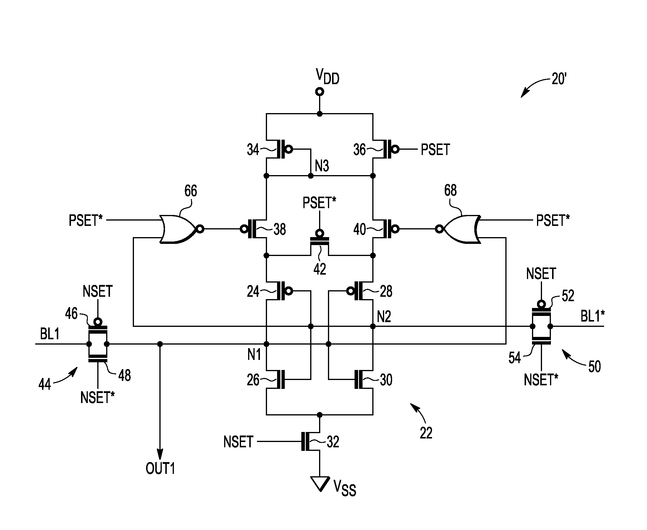
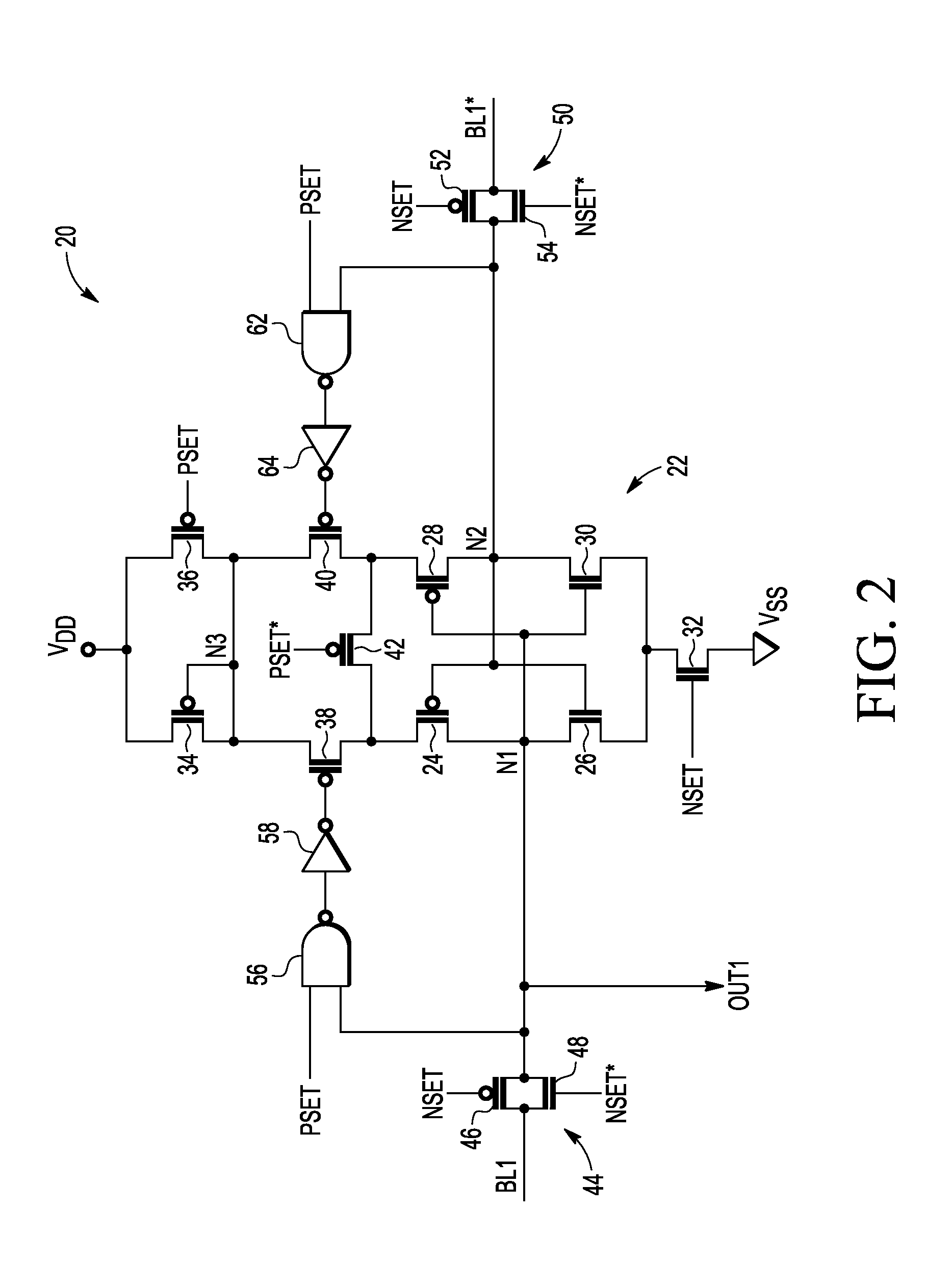
[0010]Generally, there is provided, a latching sense amplifier that is resistant to NBTI. The latching sense amplifier includes a cross-coupled latch having first and second inverters coupled between two storage nodes. Each inverter includes a P-channel transistor and an N-channel coupled together in series. A first NBTI compensation transistor has a source terminal coupled to a power supply voltage terminal. The first NBTI compensation transistor also has a drain terminal coupled to a source terminal of the P-channel transistor of the first inverter. A second NBTI transistor has a source terminal coupled to the power supply voltage terminal. The second NBTI transistor has a drain terminal coupled to a source terminal of the P-channel transistor of the second inverter. The first and second NBTI transistors are responsive to the logic states of the two storage nodes. A third NBTI compensation transistor is coupled between the drain terminals of the first and second NBTI compensation ...


PUM


Abstract

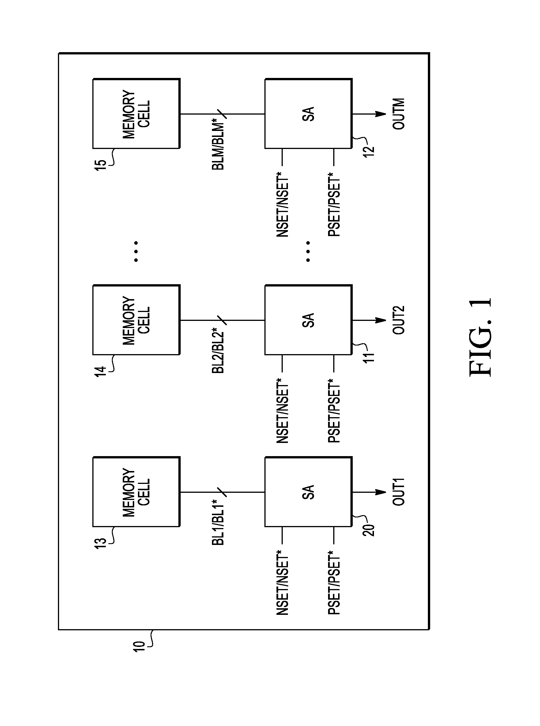
An integrated circuit includes a memory cell and a sense amplifier coupled to the memory cell via a first bit line and a second bit line. The sense amplifier includes first and second inverters cross-coupled to provide a latch. The first inverter is responsive to a first data signal provided by the memory cell over the first bit line. The second inverter is responsive to a second data signal as provided by the memory cell over the second bit line. A first negative bias temperature instability (NBTI) compensation transistor includes a source electrode coupled to receive a reference voltage, a drain electrode coupled to a source electrode of the first inverter, and a gate electrode coupled to first logic responsive to the first data signal. A second NBTI compensation transistor includes a source electrode coupled to receive the reference voltage, a drain electrode coupled to a source electrode of the second inverter, and a gate electrode coupled to second logic responsive to the second data signal, wherein the second data signal is a logical complement of the first data signal.

Description

BACKGROUND[0001]1. Field[0002]This disclosure relates generally to integrated circuit memory, and more specifically, to a memory having a latching sense amplifier resistant to negative bias temperature instability (NBTI) and method therefor.[0003]2. Related Art[0004]A one-time programmable (OTP) memory is a type of memory that is used to permanently store programs or data in integrated circuit applications. An OTP memory cell may be implemented using, for example, fuses or antif uses. Read disturb can occur in an OTP memory cell as a result of read current being repeatedly applied to the OTP memory cell, such as an electrically programmable fuse or antif use, and thus causing a stress condition in the OTP memory cell. Repeated read current stress can progressively alter the logic state of an OTP memory cell, and after a long time period move the cell from an unprogrammed state to a programmed state, causing an error. It is therefore desirable to read the OTP memory cell as little as...

Claims


Application Information

Patent Timeline
IPC IPC(8): H03F3/16H03K3/011
CPCG11C7/04H03K3/356182H03K3/011G11C7/065G11C7/06G11C5/14G11C17/00
Inventor HOEFLER, ALEXANDER B.BURNETT, JAMES D.REMINGTON, SCOTT I.
Owner VLSI TECH LLC
Learn More