Manufacturing method of high-efficiency LED
- Summary
- Abstract
- Description
- Claims
- Application Information
AI Technical Summary
Benefits of technology
Problems solved by technology
Method used
Image

Examples
Embodiment Construction
[0028]The disclosure is directed to a high-efficiency LED structure and a process thereof. To fully disclose the embodiments of the disclosure, detailed steps and compositions are described in the following embodiments. Obviously, the implementation of the disclosure in the following embodiments is not limited to special details known by persons skilled in the LED field. On the other hand, the details regarding known compositions or steps are omitted, so as to provide clear explanations for each of the embodiments In addition to the detailed description, the disclosure may be also widely applied in other embodiments, and the scope of the disclosure is not limited as defined by the appended claims.
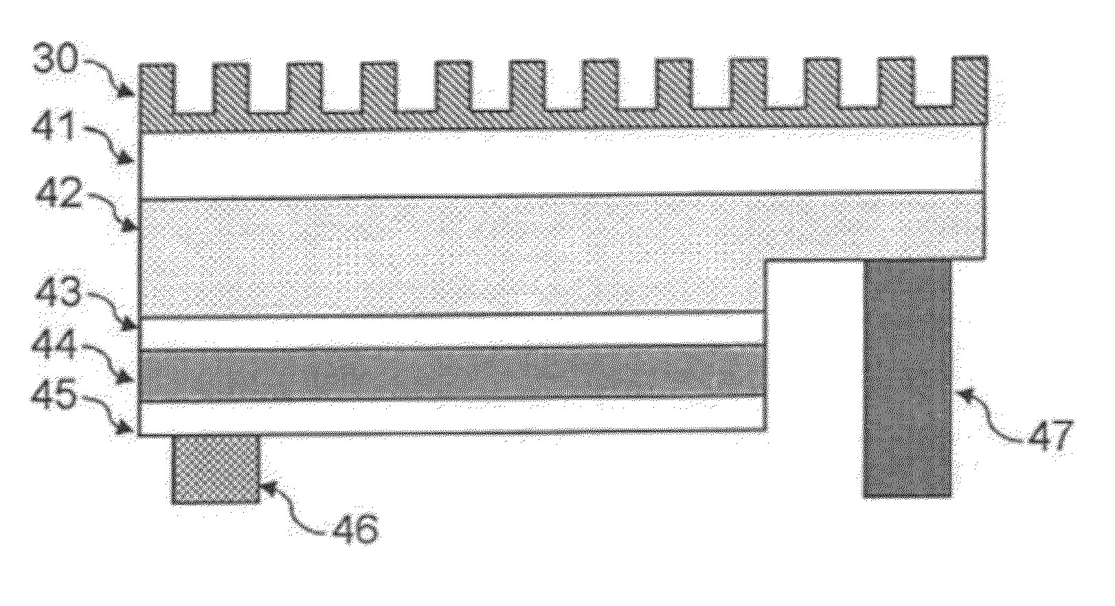
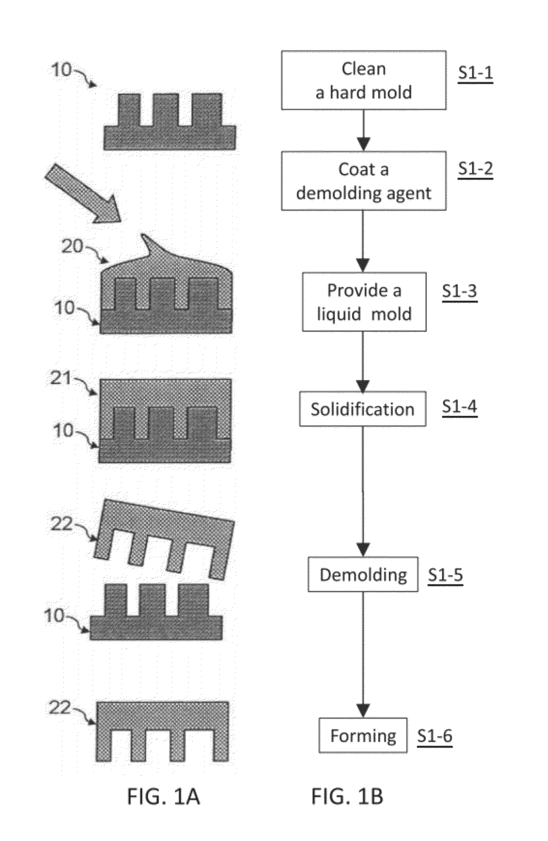
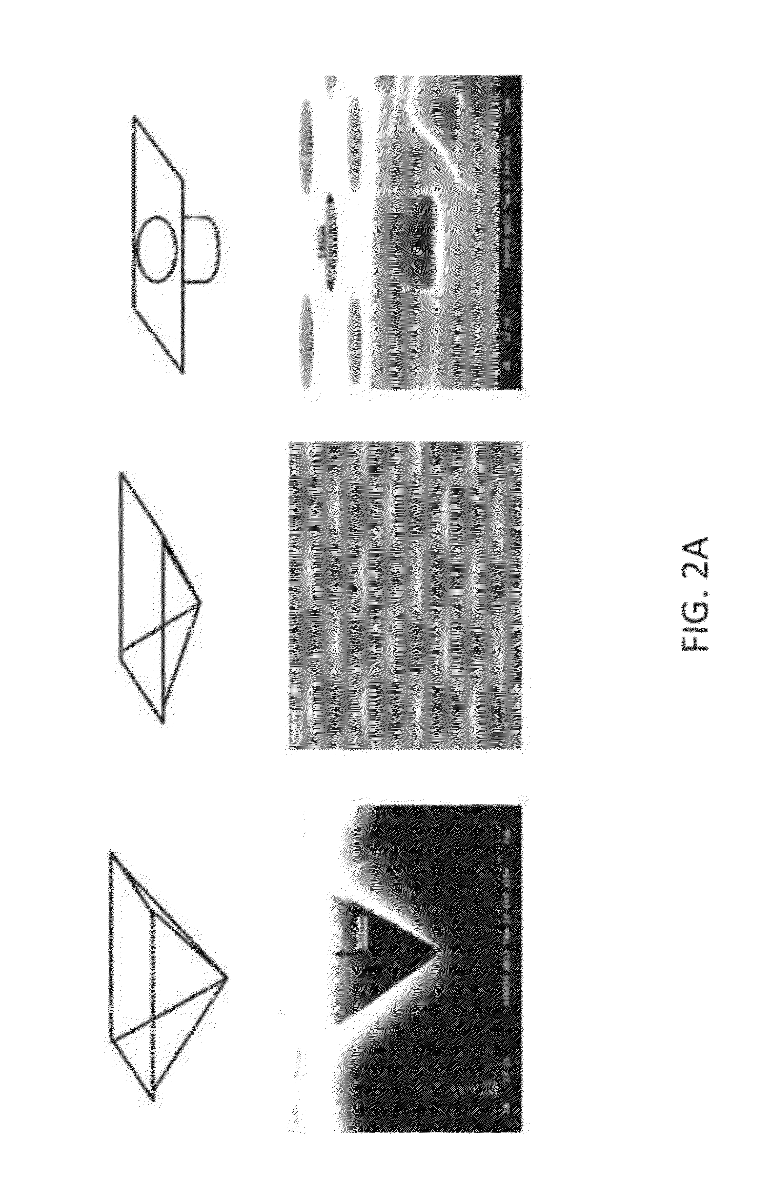
[0029]It is proved that surface structure technology can effectively improve light emitting efficiency of an LED. An embodiment of the disclosure adopts soft imprinting technology in cooperation with a reverse imprinting technology to form a micro / nano-scale structure on a camber LED wafer ...
PUM
| Property | Measurement | Unit |
|---|---|---|
| Structure | aaaaa | aaaaa |
| Microstructure | aaaaa | aaaaa |
| Efficiency | aaaaa | aaaaa |
Abstract
Description
Claims
Application Information
 - Generate Ideas
- Intellectual Property
- Life Sciences
- Materials
- Tech Scout
- Unparalleled Data Quality
- Higher Quality Content
- 60% Fewer Hallucinations
Browse by: Latest US Patents, China's latest patents, Technical Efficacy Thesaurus, Application Domain, Technology Topic, Popular Technical Reports.
© 2025 PatSnap. All rights reserved.Legal|Privacy policy|Modern Slavery Act Transparency Statement|Sitemap|About US| Contact US: help@patsnap.com