Super-junction semiconductor device
- Summary
- Abstract
- Description
- Claims
- Application Information
AI Technical Summary
Benefits of technology
Problems solved by technology
Method used
Image

Examples
first embodiment
[0036]Many conventional methods employed for preventing a super-junction semiconductor device from breaking down as a result of an overcurrent detect the overcurrent flowing through the super-junction semiconductor device. When the detected overcurrent is high enough to breakdown the super-junction semiconductor device, the conventional methods feedback the detected overcurrent to the gate signal of the main device to control the current flowing through the main device and to prevent the main device from breaking down.
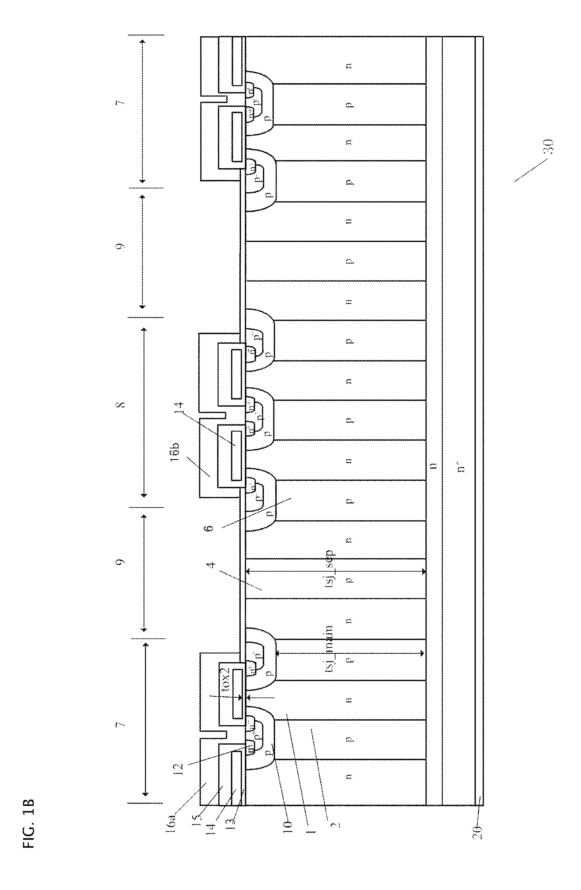
[0037]FIG. 8 is an equivalent circuit diagram, in which overcurrent protecting circuit 36 is connected to super-junction semiconductor device 30 according to the invention including main device 31 and sensing device 32.
[0038]In the equivalent circuit shown in FIG. 8, the voltage VS detected, when an overcurrent flows from the super-junction semiconductor device 30 drain, as the potential difference across overcurrent detecting resistor 33 connected to the source side o...
second embodiment
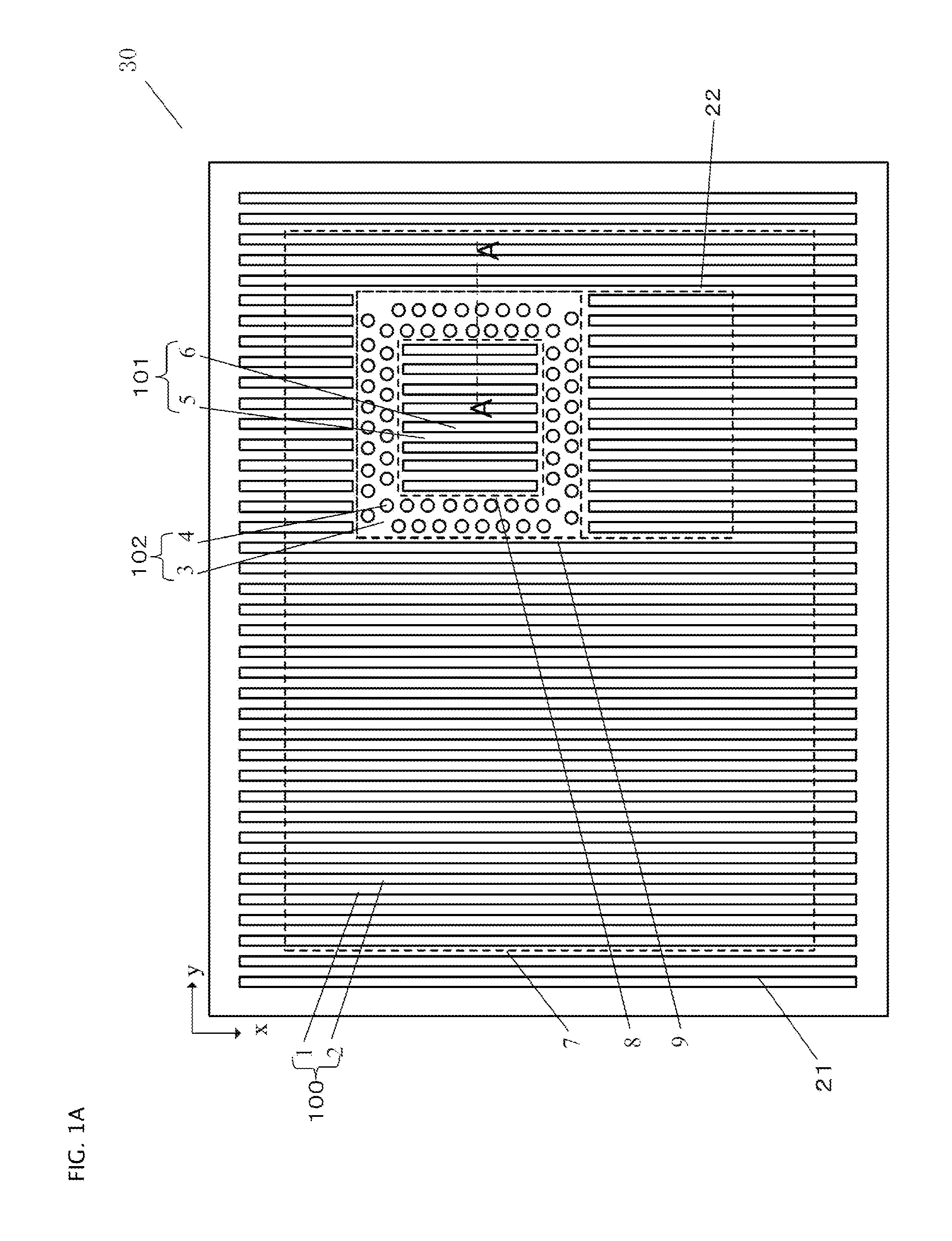
[0052]FIG. 2 is a top plan view showing the planar patterns of the alternating-conductivity-type layers in a super-junction MOSFET according to a second embodiment of the invention.
[0053]The super-junction MOSFET according to the second embodiment is a modification of the super-junction MOSFET according to the first embodiment. The super-junction MOSFET according to the second embodiment is different from the super-junction MOSFET according to the first embodiment in that the pitch of the planar lattice pattern in alternating-conductivity type layer 102 is set to be narrower than the pitch of the planar stripe pattern in alternating-conductivity type layers 100 and 101. Since the narrower pitch setting in alternating-conductivity-type layer 102 according to the second embodiment makes the depletion layers expand more easily and relaxes the electric field more easily, it is possible to obtain a higher breakdown voltage.
third embodiment
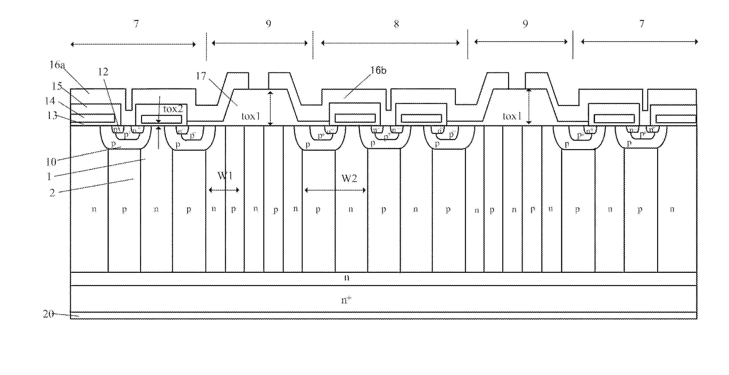
[0054]FIG. 4 is a top plan view showing the planar patterns of the alternating-conductivity-type layers in a super-junction MOSFET according to a third embodiment of the invention. FIG. 5 is the cross sectional view along the broken line C-C in FIG. 4.
[0055]For ease of understanding, the insulator films and the metal electrode films usually formed on the semiconductor chip surface of a vertical super-junction MOSFET are omitted in FIG. 4 to show the planar patterns of alternating-conductivity-type layers 100, 101, and 102 on the semiconductor substrate.
[0056]In the same manner as described in FIG. 1A, the alternating-conductivity type layers in main device region 7 and sensing device regions 8 employ a planar stripe pattern. Separation region 9 between main device region 7 and sensing device region 8 separates p-type regions 2 and 6 from each other. Sensing device region 8 is surrounded by separation region 9 on all sides. In separation region 9, p-type regions 4 are arranged in n-t...
PUM
 Abstract
Description
Claims
Application Information