Strain balanced laser diode

Inactive Publication Date: 2012-08-23
THORLABS QUANTUM ELECTRONICS
View PDF5 Cites 11 Cited by
  • Summary
  • Abstract
  • Description
  • Claims
  • Application Information

AI Technical Summary

Benefits of technology

[0006]According to the concepts of the present disclosure, laser diode waveguide configurations are contemplated where the use of Al in the waveguide layers of the laser is presented in the form of InGaN/Al(In)GaN waveguiding superstructure comprising one or more optical confining wells (InGaN) and one or more corresponding strain compensating barriers (Al(In)GaN). The composition of the optical confini

Problems solved by technology

The present inventors have also recognized that misfit defect formation is a particularly acute problem in the context of laser diode structures grown on semipolar substrates because, during the growth of AlGaN or

Method used


Image

  • Strain balanced laser diode
  • Strain balanced laser diode
  • Strain balanced laser diode

Examples


Example

EXAMPLE 1

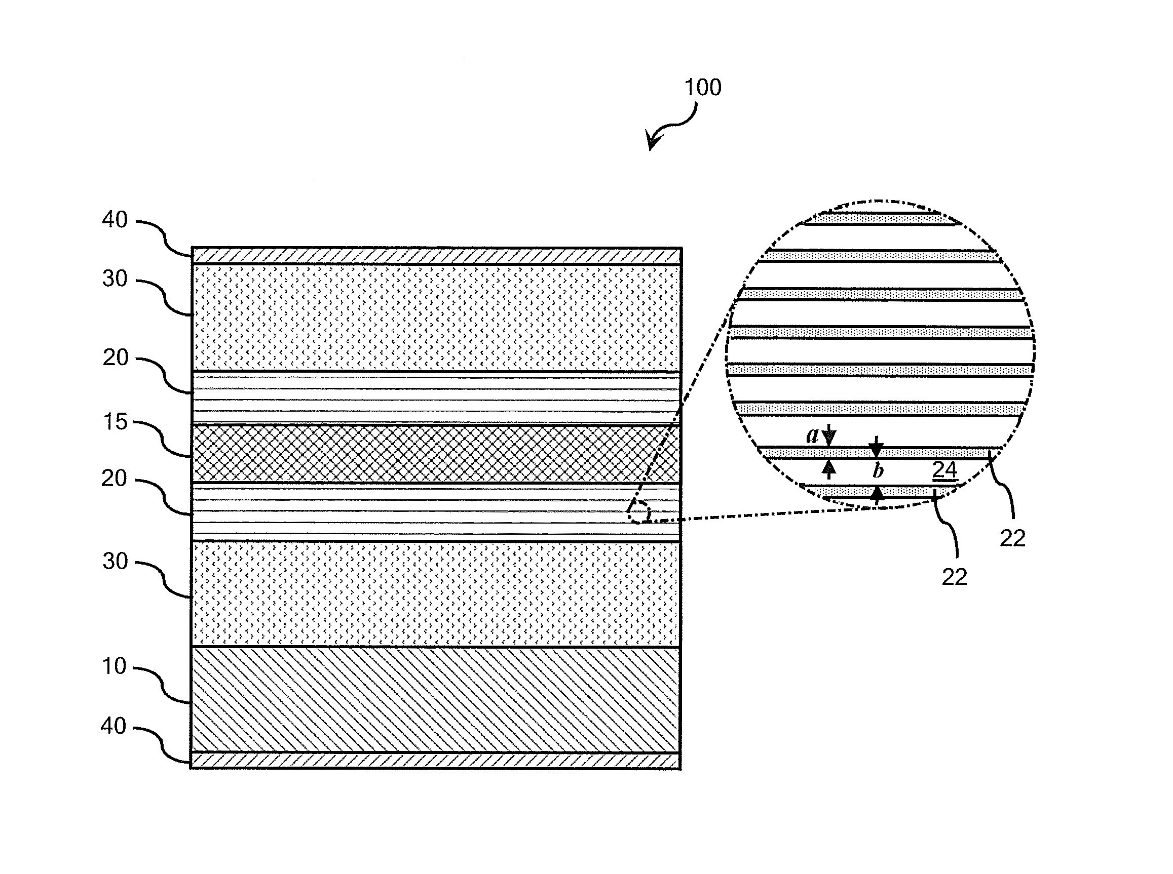
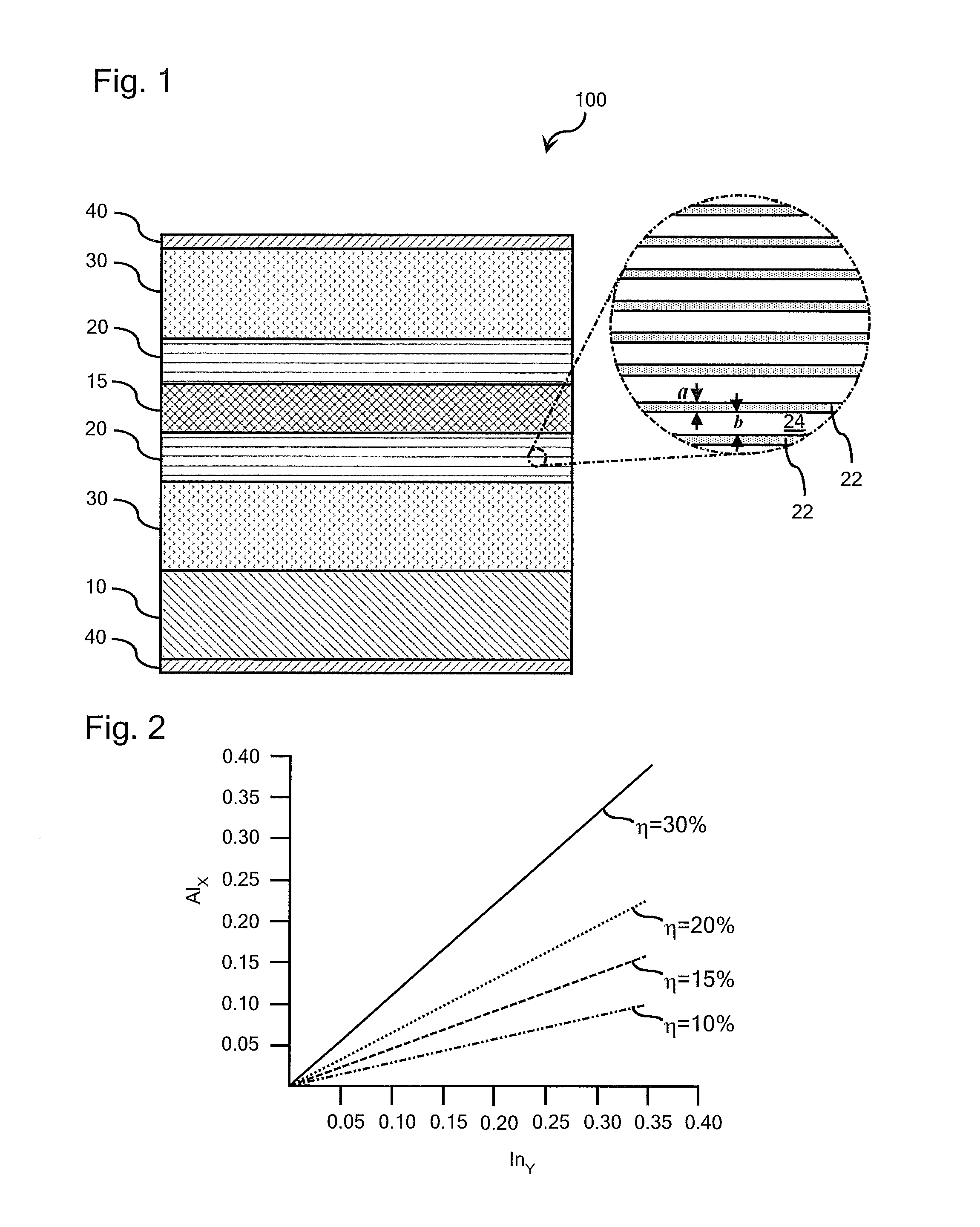
[0029]A laser diode structure comprising the following layers (from bottom to top):[0030]n-GaN buffer layer and cladding layer;[0031]8-12 periods of passive multiple quantum wells, where 2-5 nm passive QWs are separated by 10 nm AlInGaN or AlGaN barriers (for AlGaN, the Al concentration should be 5%-15%), the passive quantum wells are configured to have an emission wavelength 10-40 nm shorter than the lasing wavelength;[0032]2 or 3 periods of InGaN active quantum wells configured to provide optical gain in green spectral range (500-540 nm);[0033]AlInGaN electron blocking layer; and[0034]600-1200 nm thick p-side GaN cladding layer.

Example

EXAMPLE 2

[0035]Similar to Example 1, except an AlInGaN cladding layer is used at least in the n-side cladding layer. This AlInGaN layer lattice matched in one in-plane direction (typically toward c-axis) and has sufficiently low strain in another direction to avoid relaxation. The p-side cladding layer may comprise AlInGaN or AlGaN layer. Each cladding layer may also be made of combination of AlGaN, GaN, InGaN or AlInGaN layers. The structure can also comprise, in addition to strain compensated passive QWs, a bulk InGaN layer or InGaN / GaN superlattice in the waveguide core, to further improve optical confinement. The presence of the strain compensated passive QWs enhances optical confinement, such that high In concentration or large thickness of this bulk layers or superlattices is no longer needed and they can be thin enough to avoid relaxation. Also, due to high refractive index of the passive quantum wells, it is preferred in some designs to position the passive quantum wells bet...

Example

EXAMPLE 3

[0036]A laser diode structure comprising two passive wells with 5 nm n-AlInGaN barrier below them and 17 nm n-AlInGaN barrier above them. The two passive QWs are separated by 17 nm thick AlInGaN barrier layer. Such structure is placed between the hole blocking layer and the n-InGaN / GaN superlattice with average In concentration 3%-6%. The thickness of the n-superlattice is 114 nm, and it is below the relaxation limit for (20-21) substrate orientation. The n-AlInGaN cladding layer, or the combination of AlInGaN / GaN layers, is placed below the n-InGaN / GaN superlattice layer. The structure also comprises p-InGaN / GaN superlattice with thickness 90 nm. A p-type GaN, AlGaN, AlInGaN, or combination cladding layer may be grown similarly to examples 1 and 2. The structure should also comprise an electron blocking layer between the active region and the cladding layer.


PUM


Abstract

According to the concepts of the present disclosure, laser diode waveguide configurations are contemplated where the use of Al in the waveguide layers of the laser is presented in the form of InGaN/Al(In)GaN waveguiding superstructure comprising optical confining wells (InGaN) and strain compensating barriers (Al(In)GaN). The composition of the optical confining wells is chosen such that they provide strong optical confinement, even in the presence of the Al(In)GaN strain compensating barriers, but do not absorb lasing emission. The composition of the strain compensating barriers is chosen such that the Al(In)GaN exhibits tensile strain that compensates for the compressive strain of InGaN optical confinement wells but does not hinder the optical confinement.

Description

BACKGROUND[0001]1. Field of the Invention[0002]The present disclosure relates to semiconductor lasers and, more particularly, to an optical waveguide structure that is resistant to misfit defect formation and achieves relatively high optical confinement in the active region of the waveguide structure. Semiconductor lasers according to the present disclosure are particularly well suited, for example, as electrically pumped green laser diodes.[0003]2. Technical Background[0004]The present inventors have recognized the advantage of using semipolar substrates in the design and fabrication of electrically pumped green laser diodes based on group-III nitride compounds because of potentially higher optical gain and uniformity, particularly in the case of active regions made of InGaN quantum wells. The present inventors have also recognized that misfit defect formation is a particularly acute problem in the context of laser diode structures grown on semipolar substrates because, during the ...

Claims


Application Information

Patent Timeline
IPC IPC(8): H01S5/343
CPCB82Y20/00H01S5/2031H01S5/34333H01S5/3216H01S5/3406H01S5/3202H01S5/320275H01S5/343H01S5/32
Inventor BHAT, RAJARAMSIZOV, DMITRY S.ZAH, CHUNG-EN
Owner THORLABS QUANTUM ELECTRONICS
Why Eureka
Try Eureka