Pixel circuit and display device

a display device and pixel circuit technology, applied in the field of active matrix type display devices, can solve the problems of fluctuation of the data voltage held in the pixel electrode, and inability to provide sufficient contrast, so as to achieve the effect of not reducing the aperture rate largely and cutting power consumption

Active Publication Date: 2012-08-30
SHARP KK
View PDF1 Cites 21 Cited by
  • Summary
  • Abstract
  • Description
  • Claims
  • Application Information

AI Technical Summary

Benefits of technology

[0095]According to the pixel circuit of the present invention, the refreshing action can be executed for the plurality of arranged pixels collectively with respect to each voltage state held therein by performing the self refreshing action. Therefore, the number of times required to drive the driver circuit from the start to the end of the refreshing action can be considerably reduced, and power consumption can be cut.
[0096]Thus, since it is not necessary to separately provide a memory part such as a SRAM in the pixel circuit, the aperture rate is not largely lowered unlike the conventional technique.

Problems solved by technology

However, when the refreshing frequency is lowered, the pixel data voltage held in the pixel electrode fluctuates due to a leak current of the TFT.
In addition, since an average potential is lowered in each frame period, a display quality could be lowered such that a sufficient contrast cannot be provided.

Method used


Image

  • Pixel circuit and display device
  • Pixel circuit and display device
  • Pixel circuit and display device

Examples


first embodiment

[0138]In a first embodiment, a description will be given of configurations of the display device of the present invention (hereinafter, simply referred to as the “display device”) and the pixel circuit of the present invention (hereinafter, simply referred to as the “pixel circuit”).

[0139]>

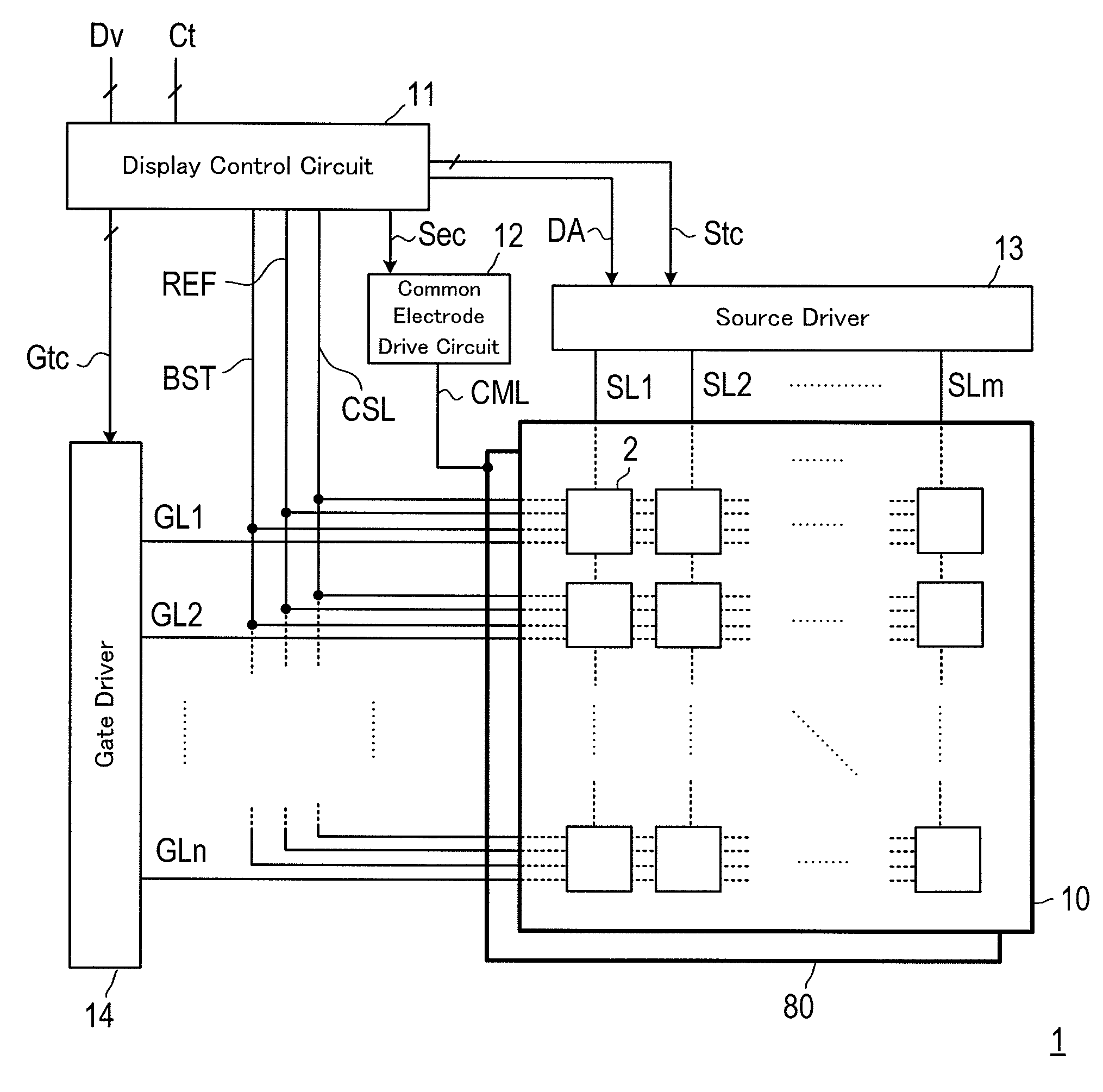
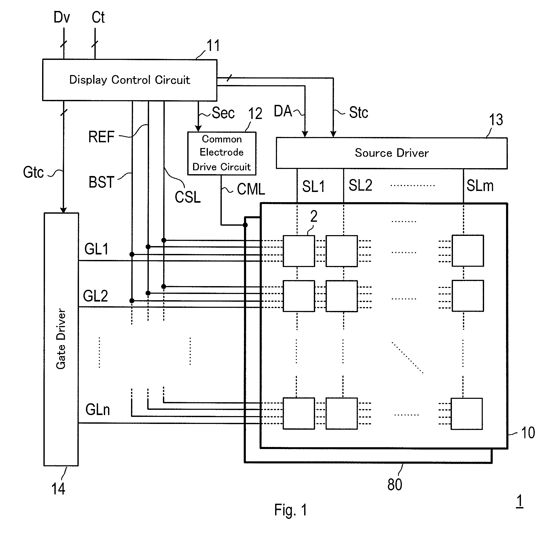
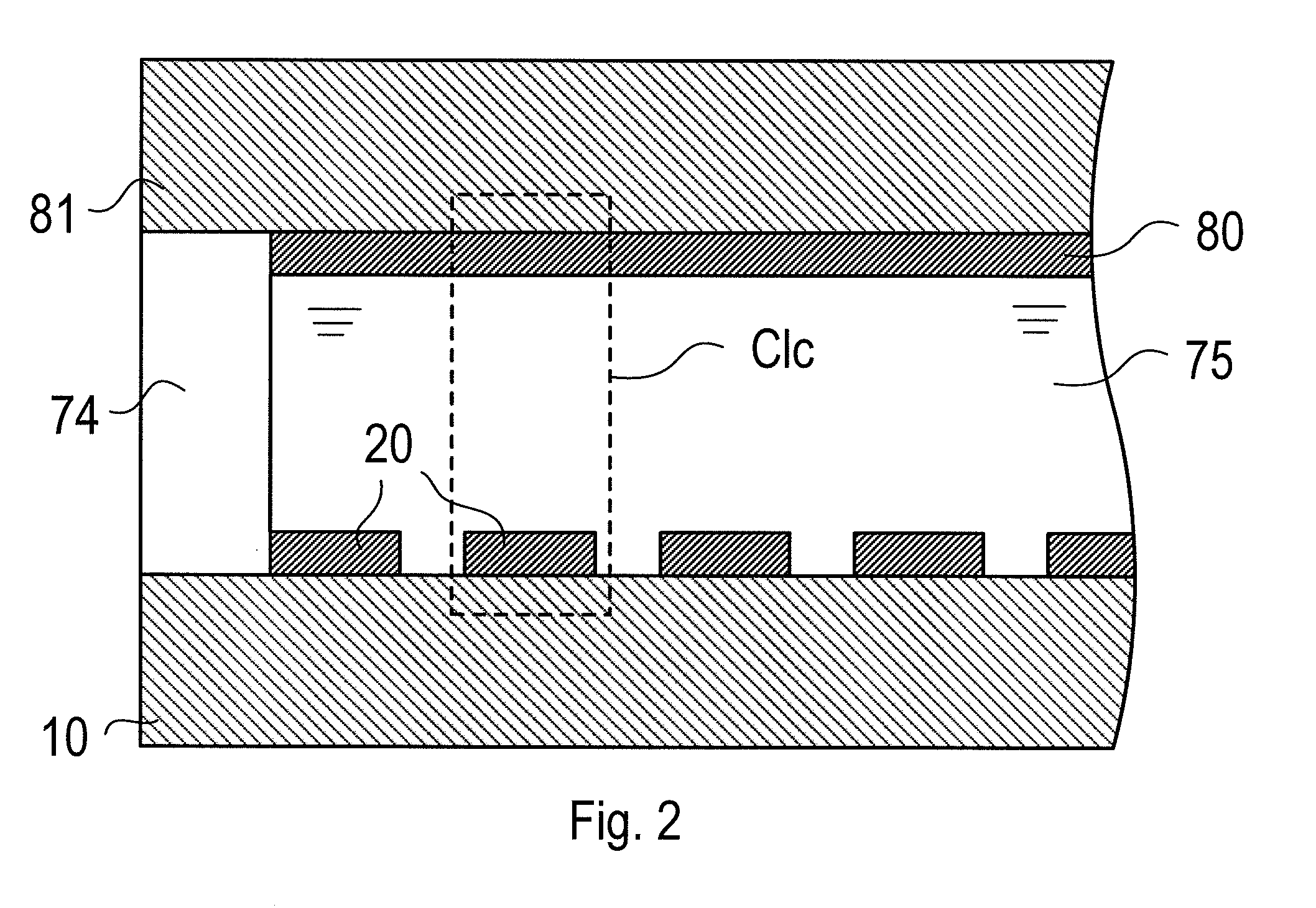
[0140]FIG. 1 shows a schematic configuration of a display device 1. The display device 1 includes an active matrix substrate 10, an opposite electrode 80, a display control circuit 11, an opposite electrode drive circuit 12, a source driver 13, a gate driver 14, and various signal lines which will be described below. On the active matrix substrate 10, a plurality of pixel circuits 2 are arranged in raw and column directions, respectively, and a pixel circuit array is formed.

[0141]In addition, the pixel circuit 2 is shown as a block in FIG. 1 so as to prevent the drawing from becoming complicated. Moreover, for descriptive purposes, the active matrix substrate 10 is shown above the opposite electro...

second embodiment

[0196]In a second embodiment, a description will be given of a self refreshing action in each of the first to third type pixel circuits with reference to the drawings.

[0197]The self refreshing action means an action in the constant display mode performed for the plurality of the pixel circuits 2 such that the first switch circuits 22, the second switch circuits 23, and the control circuits 24 are activated in a predetermined sequence, and the potentials of the pixel electrodes 20 (this is also the potentials of the internal nodes N1) are restored to a potential of the gradation written in the last writing action, and for the pixels of all gradations, the pixel circuits are collectively recovered at the same time with respect to each gradation. The self refreshing action is a specific action by the pixel circuits 2A to 2E in the present invention, and power consumption can be considerably reduced, compared to the conventional “external refreshing action” in which the potential of the...

third embodiment

[0279]In the third embodiment, a description will be given of a case where the self refreshing action is executed by a voltage application method different from that of the second embodiment, with reference to the drawings. In addition, the self refreshing action of this embodiment is divided into the refreshing step S1 and the stand-by step S2, similar to the second embodiment.

[0280]According to the second embodiment, only the internal node N1 of the case H (high voltage writing) is refreshed in the phase P1, and only the internal node N1 of the case M (middle voltage writing) is refreshed in the phase P2. Thus, in the step S1, the pulse voltage needs to be applied to the boost line BST in each of the phase P1 and phase P2.

[0281]Meanwhile, according to this embodiment, only the internal node N1 of the case M (middle voltage writing) is refreshed in the phase P1, and only the internal node N1 of the case H (high voltage writing) is refreshed in the phase P2 as will be described belo...


PUM


Abstract

A display device in which low power consumption is realized without lowering an aperture ratio is provided. A liquid crystal capacitive element Clc is sandwiched between a pixel electrode 20 and an opposite electrode 80. The pixel electrode 20, one end of a first switch circuit 22, one end of a second switch circuit 23 and a first terminal of a second transistor T2 form an internal node N1. The other terminals of the first switch circuit 22 and the second switch circuit 23 are connected to a source line SL. The second switch circuit 23 is a series circuit composed of a first transistor T1 and a diode D1. A control terminal of the first transistor T1, a second terminal of the second transistor T2 and one end of a boost capacitive element Cbst form an output node N2. The other end of the boost capacitive element Cbst and the control terminal of the second transistor T2 are connected to a boost line BST and a reference line REF, respectively. The diode D1 has a rectifying function from the source line SL to the internal node N1.

Description

REFERENCE TO RELATED APPLICATIONS[0001]This application is a National Phase filing under 35 U.S.C. §371 of International Application No. PCT / JP2010 / 068581 filed on Oct. 21, 2010, and which claims priority to Japanese Patent Applications No. 2009-248964 filed on Oct. 29, 2009, No. 2010-094029 filed on Apr. 15, 2010, and No. 2010-228756 filed on Oct. 8, 2010.FIELD OF THE INVENTION[0002]The present invention relates to a pixel circuit and a display device provided with the same, and more particularly to an active matrix type display device.BACKGROUND OF THE INVENTION[0003]A mobile terminal such as a mobile telephone or a mobile game machine uses a liquid crystal display device as its displaying means, in general. In addition, since the mobile telephone is driven by a battery, it is strongly required to reduce power consumption. Therefore, information such as a time or remaining battery level which needs to be constantly displayed is displayed on a reflective subpanel. In addition, rece...

Claims


Application Information

Patent Timeline
Patent Type & Authority Applications(United States)
IPC IPC(8): G09G5/00
CPCG02F1/13624G09G3/3655G09G3/3659G09G3/3618G09G2300/0814G09G2300/0876G09G3/367
Inventor UEDA, NAOKIYAMAUCHI, YOSHIMITSUNAKANO, FUMIKI
Owner SHARP KK
Why Eureka
Try Eureka