Thermal Anneal of Block Copolymer Films with Top Interface Constrained to Wet Both Blocks with Equal Preference

a technology of copolymer and top interface, which is applied in the field of self-assembling block copolymer thin film fabrication, can solve the problems of difficult fabrication of structures and features at the sub-60 nanometer level and the difficulty of optical lithographic processing methods in achieving the effect of sub-60 nanometers and a fast process

Active Publication Date: 2012-09-06
MICRON TECH INC
View PDF5 Cites 54 Cited by
  • Summary
  • Abstract
  • Description
  • Claims
  • Application Information

AI Technical Summary

Problems solved by technology

Making electrical contacts to conductive lines has become a significant challenge as the dimensions of semiconductor features shrink to sizes that are not easily accessible by conventional lithography.
Optical lithographic processing methods have difficulty fabricating structures and features at the sub-60 nanometer level.
Solvent annealing of BCPs has been used to produce a perpendicular orientation of the self-assembled domains to the substrate, but is generally a very slow process, typically on the order of days, and can require large volumes of the solvent.

Method used


Image

  • Thermal Anneal of Block Copolymer Films with Top Interface Constrained to Wet Both Blocks with Equal Preference
  • Thermal Anneal of Block Copolymer Films with Top Interface Constrained to Wet Both Blocks with Equal Preference
  • Thermal Anneal of Block Copolymer Films with Top Interface Constrained to Wet Both Blocks with Equal Preference

Examples


Embodiment Construction

[0017]The following description with reference to the drawings provides illustrative examples of devices and methods according to embodiments of the invention. Such description is for illustrative purposes only and not for purposes of limiting the same.

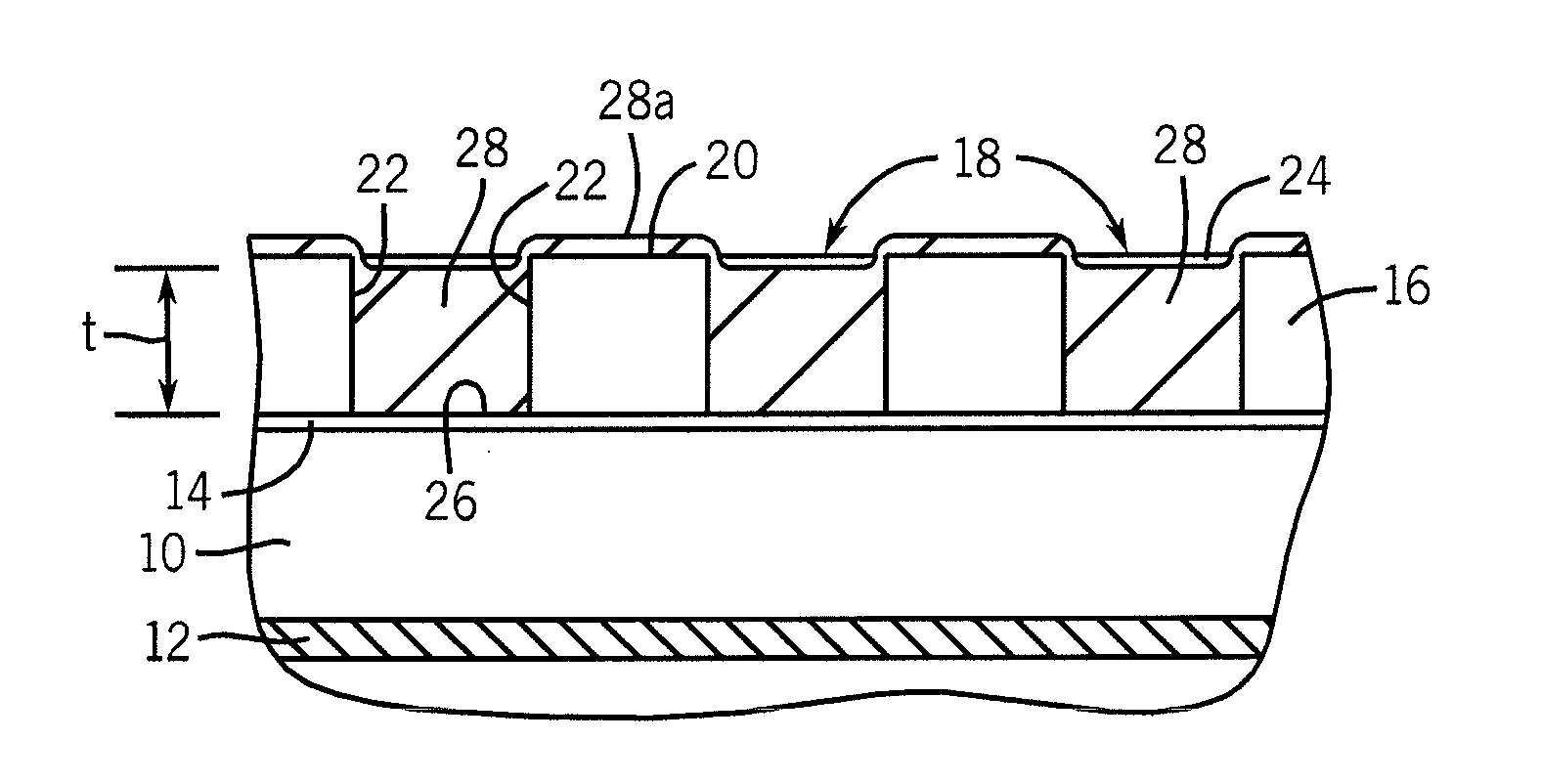
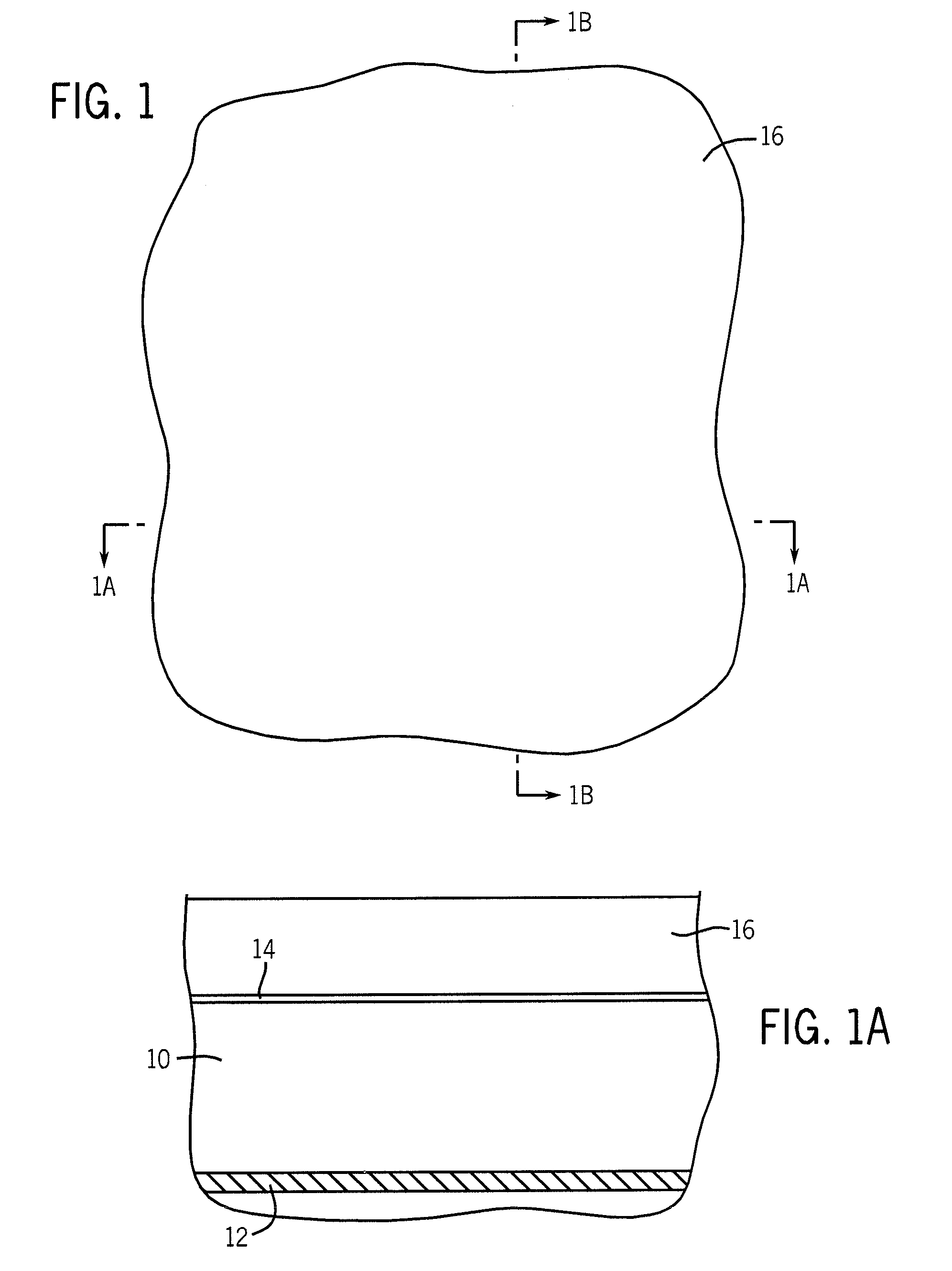
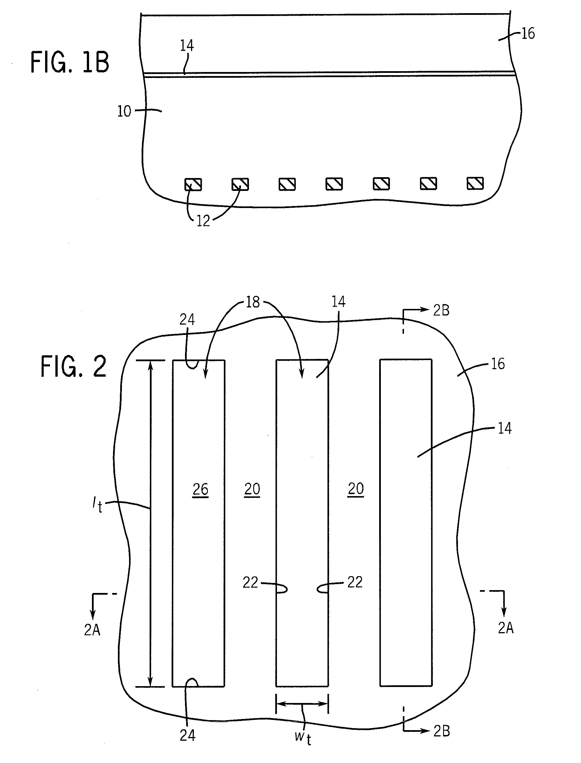
[0018]In the context of the current application, the term “semiconductor substrate” or “semiconductive substrate” or “semiconductive wafer fragment” or “wafer fragment” or “wafer” will be understood to mean any construction comprising semiconductor material, including but not limited to bulk semiconductive materials such as a semiconductor wafer (either alone or in assemblies comprising other materials thereon), and semiconductive material layers (either alone or in assemblies comprising other materials). The term “substrate” refers to any supporting structure including, but not limited to, the semiconductive substrates, wafer fragments or wafers described above.

[0019]“Lo” as used herein is the inherent periodicity or pitch value (bul...


PUM

PropertyMeasurementUnit
feature sizeaaaaaaaaaa
widthaaaaaaaaaa
widthaaaaaaaaaa

Abstract

Methods for fabricating sublithographic, nanoscale microstructures utilizing self-assembling block copolymers, and films and devices formed from these methods are provided.

Description

CROSS-REFERENCE TO RELATED APPLICATION[0001]This application is a continuation of U.S. Ser. No. 12 / 052,956, filed Mar. 21, 2008.TECHNICAL FIELD[0002]Embodiments of the invention relate to methods of fabricating thin films of self-assembling block copolymers, and devices resulting from those methods.BACKGROUND OF THE INVENTION[0003]As the development of nanoscale mechanical, electrical, chemical and biological devices and systems increases, new processes and materials are needed to fabricate nanoscale devices and components. Making electrical contacts to conductive lines has become a significant challenge as the dimensions of semiconductor features shrink to sizes that are not easily accessible by conventional lithography. Optical lithographic processing methods have difficulty fabricating structures and features at the sub-60 nanometer level. The use of self assembling diblock copolymers presents another route to patterning at nanoscale dimensions. Diblock copolymer films spontaneou...

Claims


Application Information

Patent Timeline
Patent Type & Authority Applications(United States)
IPC IPC(8): B44C1/22C08L75/04C08L83/04C08F212/08C08G65/34
CPCB81C1/00031B81C2201/0149B81C2201/0198C08F299/0492H01L21/0337H01L21/0338C08F299/02B82Y30/00G03F7/0002H01L21/76816H01L21/0275B81C2201/013H01L21/31133H01L21/76802H01L21/76828H01L21/76877
Inventor MILLWARD, DAN B.QUICK, TIMOTHY
Owner MICRON TECH INC
Why Eureka
Try Eureka