Semiconductor memory device and method for manufacturing the same

a memory device and semiconductor technology, applied in the direction of semiconductor devices, electrical appliances, transistors, etc., can solve the problems of large power consumption, deterioration of transistors, and significant problems, so as to reduce oxygen vacancy, reduce the off-state current of the transistor, and reduce the oxygen vacancy

Inactive Publication Date: 2012-09-06
SEMICON ENERGY LAB CO LTD
View PDF6 Cites 27 Cited by
  • Summary
  • Abstract
  • Description
  • Claims
  • Application Information

AI Technical Summary

Benefits of technology

[0023]Note that when an oxide semiconductor film is used for the channel region in the transistor, the off-state current of the transistor can be reduced. Here, the off-state current refers to a current corresponding to electric charge moving between a source electrode and a drain electrode in a state where no voltage is applied between a gate electrode and the source electrode in the transistor.
[0024]For the oxide semiconductor film, a material having a band gap of 2.5 eV or more, preferably 3.0 eV or more may be selected. With use of a material with a band gap in the above range, the off-state current of the transistor can be reduced. Note that in one embodiment of the present invention, another material having semiconductor characteristics and a band gap in the above range may be applied.
[0025]It is preferable that the oxide semiconductor film be highly purified so as to contain as little impurities (such as hydrogen, an alkali metal, an alkaline earth metal, a rare gas, nitrogen, phosphorus, or boron) causing carriers directly or indirectly as possible. Furthermore, it is preferable to reduce oxygen vacancy as much as possible. By reducing impurities and oxygen vacancy in the oxide semiconductor film, generation of carriers in the oxide semiconductor film is suppressed, and the off-state current of the transistor can be reduced.
[0026]As described above, with the transistor with small off-state current, retention characteristic of charge accumulated in a capacitor in a DRAM can be improved. As a result, frequency of refresh operation and the area of the capacitor can be reduced.
[0027]A semiconductor memory device in which power consumption is lowered by decreasing the number of refresh operation for holding data is provided.
[0028]A semiconductor memory device in which with a channel region formed in accordance with a shape of a groove portion in a transistor, the influence caused by the short-channel effect is reduced even when the integration degree is increased is provided. In manufacturing such a semiconductor memory device, the number of steps in photolithography is smaller than that of photolithography needed for manufacturing a conventional device.

Problems solved by technology

A conventional DRAM needs to be refreshed at an interval of several tens of milliseconds to hold data, which results in large power consumption.
In addition, a transistor therein is frequently turned on and off; thus, deterioration of the transistor is also a problem.
These problems become significant as the memory capacity increases and transistor miniaturization advances.

Method used


Image

  • Semiconductor memory device and method for manufacturing the same
  • Semiconductor memory device and method for manufacturing the same
  • Semiconductor memory device and method for manufacturing the same

Examples


embodiment 1

[0048]In this embodiment, a transistor included in a semiconductor memory device according to one embodiment of the present invention will be described.

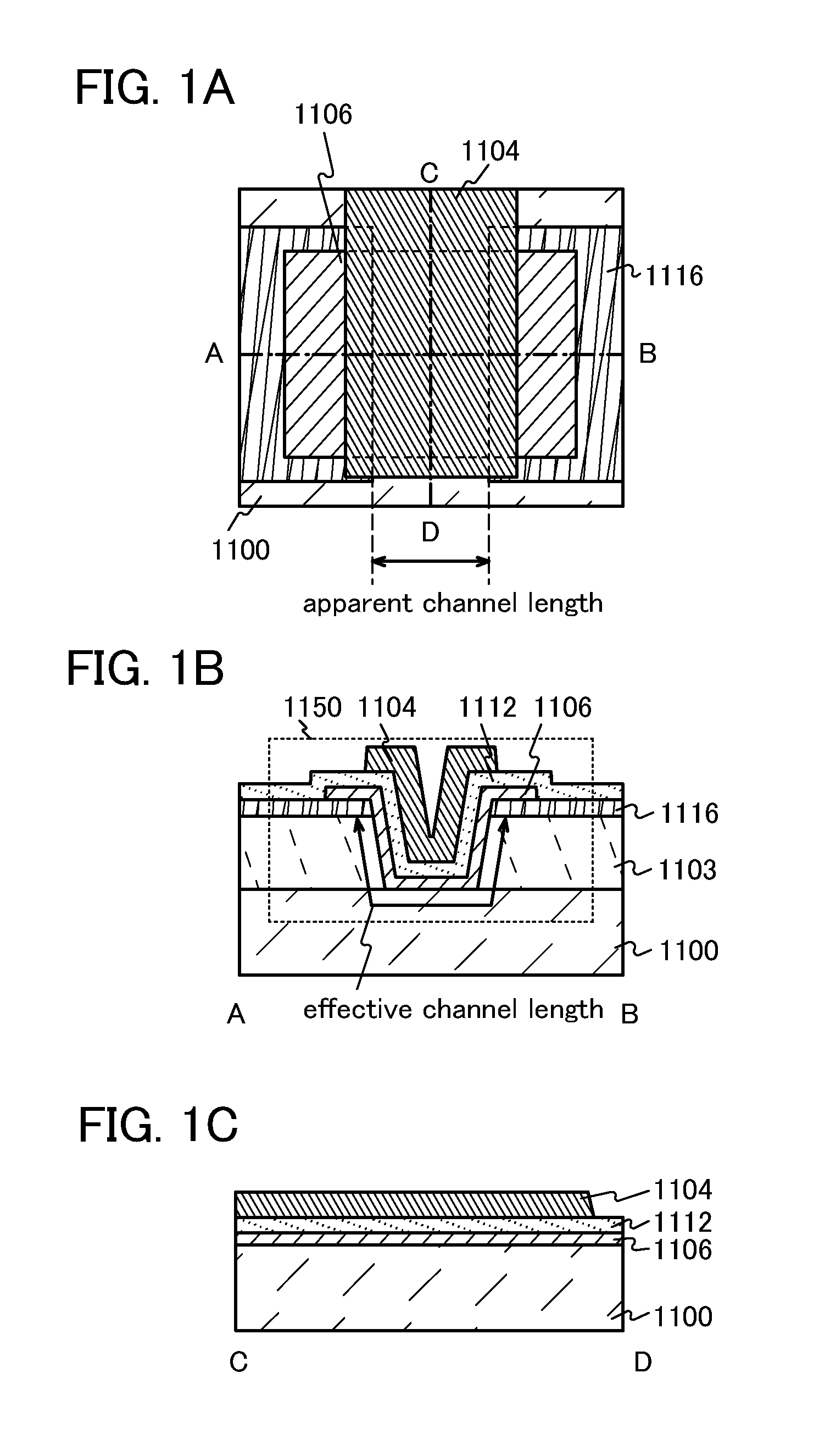
[0049]FIG. 1A is a top view of a transistor 1150. FIG. 1B illustrates a cross section A-B along dashed-dotted line A-B in FIG. 1A, and FIG. 1C illustrates a cross section C-D along dashed-dotted line C-D in FIG. 1A.

[0050]The transistor 1150 includes: a pair of electrodes 1116 over a substrate 1100 having an insulating surface; an insulating film 1103 which is below the pair of electrodes 1116 and substantially aligned with the pair of electrodes 1116 as viewed from above; an oxide semiconductor film 1106 in contact with the pair of electrodes 1116, side surfaces of the insulating film 1103, and a surface of the substrate 1100; a gate insulating film 1112 covering the oxide semiconductor film 1106; and a gate electrode 1104 provided over the oxide semiconductor film 1106 with the gate insulating film 1112 positioned therebetween.

[0051...

embodiment 2

[0097]In this embodiment, a circuit configuration of a DRAM that is a semiconductor memory device to which one embodiment of the present invention is applied will be described, and structures of a transistor and a capacitor included in the DRAM will also be described.

[0098]FIG. 6 illustrates a memory cell array including a plurality of memory cells arranged in a matrix including n rows and m columns, to which DRAMs are applied. Each memory cell includes one transistor and one capacitor. Bit lines and word lines are connected to the memory cells. Of each transistor, one of a source electrode and a drain electrode is connected to the bit line, and a gate electrode is connected to the word line. Further, the other of the source electrode and the drain electrode of the transistor is connected to one of electrodes in the capacitor. The other electrode in the capacitor is connected to the ground (GND). The bit lines are also connected to sense amplifiers.

[0099]FIG. 7A illustrates an examp...

embodiment 3

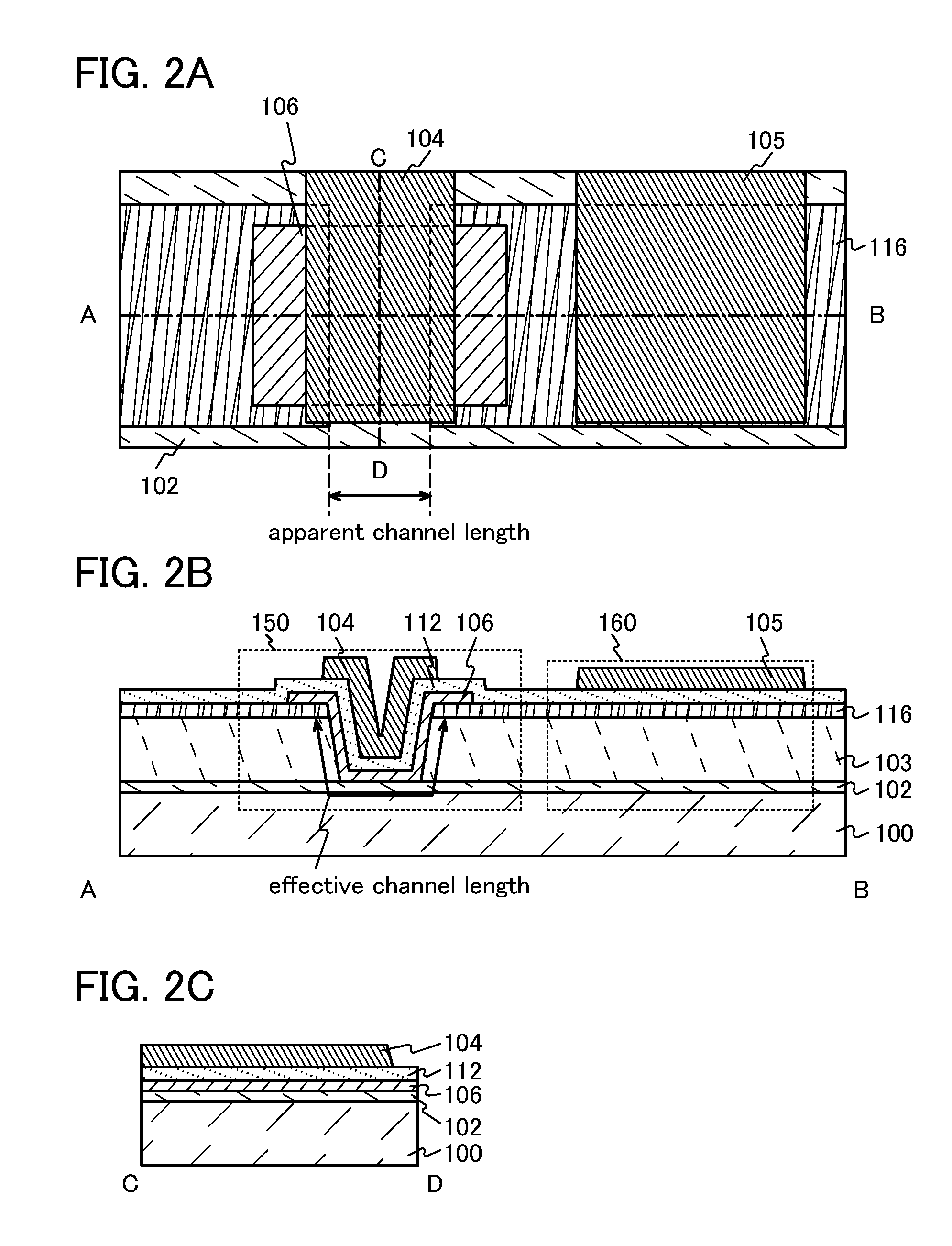
[0128]FIGS. 3A to 3C are a top view and cross-sectional views illustrating a transistor 250 and a capacitor 260 which respectively correspond to the transistor Tr and the capacitor C included in the memory cell CL. FIG. 3B illustrates a cross section A-B along dashed-dotted line A-B in FIG. 3A, and FIG. 3C illustrates a cross section C-D along dashed-dotted line C-D in FIG. 3A.

[0129]A semiconductor memory device includes the transistor 250 and the capacitor 260. The transistor 250 includes: a substrate 200; a base insulating film 202 over the substrate 200; an insulating film 203 provided over the base insulating film 202 and having a groove portion; a pair of electrodes 216 which is provided over the insulating film 203 and substantially aligned with one side surface of the insulating film 203 viewed from above; an oxide semiconductor film 206 in contact with the pair of electrodes 216 and side surfaces and a bottom surface of the groove portion formed in the insulating film 203; a...


PUM


Abstract

A semiconductor memory device includes a transistor and a capacitor. The transistor includes: an insulating film in which a groove portion is provided; a pair of electrodes separated so that the groove portion is sandwiched therebetween; an oxide semiconductor film which is in contact with the pair of electrodes and side surfaces and a bottom surface of the groove portion and has a thickness value smaller than a depth value of the groove portion; a gate insulating film covering the oxide semiconductor film; and a gate electrode provided to overlap with the oxide semiconductor film with the gate insulating film positioned therebetween.

Description

BACKGROUND OF THE INVENTION[0001]1. Field of the Invention[0002]The present invention relates to a semiconductor memory device which includes a circuit including a semiconductor element such as a transistor.[0003]2. Description of the Related Art[0004]A dynamic random access memory (DRAM) is a semiconductor memory device where one bit of data can be stored with use of one transistor and one capacitor. The DRAM has advantages such as a small area per unit memory cell, easiness in integration for modularization, and low manufacturing cost.[0005]Circuit patterns for DRAMs, like those for other semiconductor integrated circuits, have been miniaturized in accordance with the scaling law, and there was a time when it was considered difficult to achieve a design rule of 100 nm or less. One of the reasons is that in a transistor having a channel length of 100 nm or less, a leakage current caused by a punch-through phenomenon is likely to flow due to a short-channel effect and the transistor...

Claims


Application Information

Patent Timeline
Patent Type & Authority Applications(United States)
IPC IPC(8): H01L29/786H01L21/20
CPCH01L21/02554H01L21/02565H01L27/10805H01L29/78696H01L27/1225H01L29/42384H01L29/7869H01L27/10873H10B12/30H10B12/05H10B12/038H10B12/053
Inventor NODA, KOSEIENDO, YUTA
Owner SEMICON ENERGY LAB CO LTD
Why Eureka
Try Eureka