Vibrating device, method for manufacturing vibrating device, and electronic apparatus

a vibrating device and electronic equipment technology, applied in the manufacture of cables/conductor parts, basic electric elements, generators/motors, etc., can solve the problems of reducing the cost of vibrating devices, requiring relatively high cost for renewing packages, and requiring relatively high cost, etc., to achieve excellent sensitivity or oscillation characteristics, low cost, and easy-to-deal

Inactive Publication Date: 2012-09-06
SEIKO EPSON CORP
View PDF8 Cites 25 Cited by
  • Summary
  • Abstract
  • Description
  • Claims
  • Application Information

AI Technical Summary

Benefits of technology

[0052]The electronic apparatus having the configuration includes the vibrating device of the application example or the vibrating device manufactured by the manufacturing method of the application example, that is, the vibrating device which easily deals with the design change of the semiconductor circuit element or the vibrating reed and is low in cost, or the vibrating device which has excellent sensitivity or oscillation characteristics and high reliability. Therefore, the electronic apparatus has high functionality, and a reduction in cost can be achieved.

Problems solved by technology

However, ceramic packages are generally expensive, which is a bottleneck in reducing the cost of the vibrating devices.
Especially in the design change of an IC chip or a sensor element, there is a problem that a relatively high cost is needed in renewing the package.
Moreover, since package manufacturers capable of dealing with miniaturization and refinement for meeting the increased needs for the miniaturization of electronic apparatuses in recent years are limited, there is a problem that it is hard to obtain ceramic packages dealing with the miniaturization.

Method used


Image

  • Vibrating device, method for manufacturing vibrating device, and electronic apparatus
  • Vibrating device, method for manufacturing vibrating device, and electronic apparatus
  • Vibrating device, method for manufacturing vibrating device, and electronic apparatus

Examples


first embodiment

Sensor Device

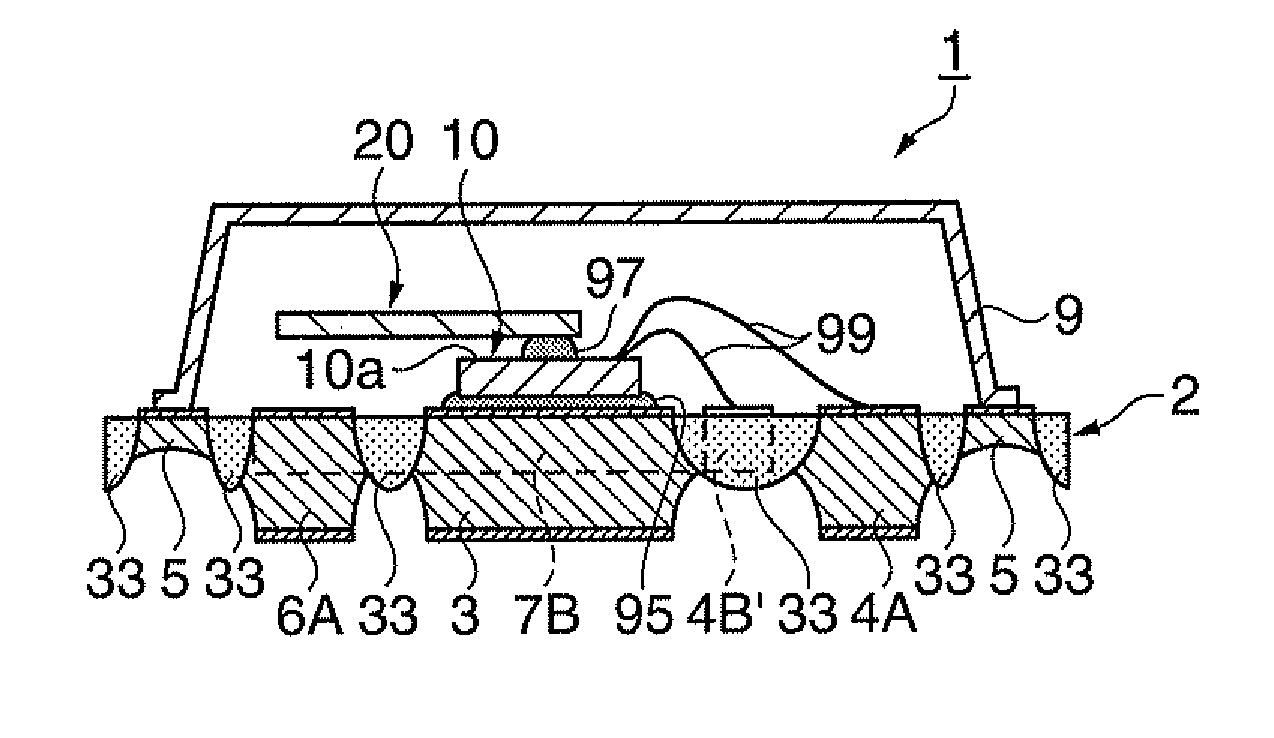
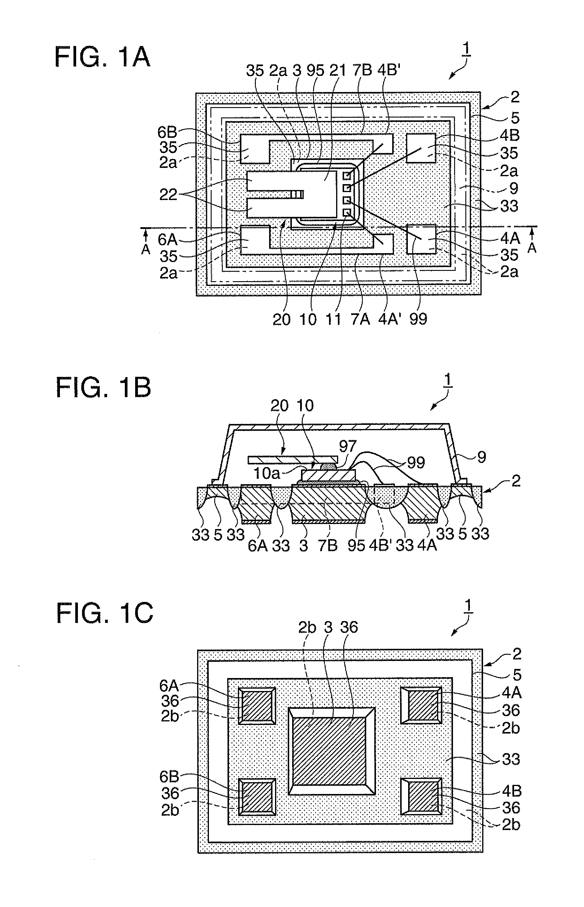
[0066]FIGS. 1A to 1C are schematic views showing a schematic configuration of a first embodiment of a sensor device as a vibrating device, in which FIG. 1A is a plan view viewed from the side (upper side) of an IC chip as a semiconductor circuit element, FIG. 1B is a cross-sectional view along line A-A of FIG. 1A, and FIG. 1C is a plan view viewed from the side (lower side) of a bottom face.

[0067]In FIGS. 1A to 1C, the sensor device 1 has a substrate 2, an IC chip 10, a sensor element 20 as a vibrating reed, and a lid 9. The substrate 2 includes a plurality of metal posts and an insulator 33 which integrally fixes the metal posts in a state of being electrically independent of each other. The IC chip 10 and the sensor element 20 are mounted on the substrate 2. The lid 9 is disposed so as to cover the IC chip 10 and the sensor element 20.

[0068]The substrate 2 includes the plurality of metal posts which are formed by performing an etching process on a metal plate having a...

second embodiment

[0130]Hereinafter, a second embodiment of a sensor device will be described.

[0131]FIG. 6 is a schematic view showing a schematic configuration of the second embodiment of the sensor device. The schematic view is a cross-sectional view showing the same section as that of FIG. 1B.

[0132]The sensor device of the second embodiment has the same configuration as that of the sensor device 1 of the first embodiment, other than plated layers formed on a first face and a second face of a substrate. Therefore, portions in common with those in the first embodiment are denoted by the same reference and numeral signs, and the description thereof is omitted.

[0133]In FIG. 6, the sensor device 101 of the second embodiment has a substrate 102 including a plurality of metal posts and the insulator 33 which integrally fixes the metal posts in a state of being electrically independent of each other, the IC chip 10 and the sensor element 20 which are mounted on the substrate 102, and the lid 9 which seals...

modified example

[0154]Hereinafter, a modified example of a sensor device will be described with reference to the drawings.

[0155]FIGS. 10A and 10B are schematic views showing a schematic configuration of the modified example of the sensor device, in which FIG. 10A is a plan view viewed from the side (upper side) of an IC chip and FIG. 10B is a cross-sectional view along line B-B of FIG. 10A. Portions in common with those of the embodiment are denoted by the same reference and numeral signs, and the description thereof is omitted. Configurations different from the embodiment will be mainly described.

[0156]The sensor device 201 of the modified example shown in FIGS. 10A and 10B has a substrate 202 including a plurality of metal posts and the insulator 33 which integrally fixes the metal posts in a state of being electrically independent of each other, the IC chip 10 and the sensor element 20 which are mounted on the substrate 202, and a plate-like lid 209 which seals the IC chip 10 and the sensor elem...


PUM


Abstract

A sensor device includes a substrate, an IC chip, a sensor element, bonding wires, and a lid. The substrate includes a plurality of metal posts which are disposed so as to be electrically independent of each other and an insulator which is filled in a gap between faces different from first faces and second faces of the plurality of metal posts and integrally fixes the plurality of metal posts. The IC chip has electrode pads on an active face and is fixed to a first metal post. The sensor element has vibrating portions and is supported by the IC chip by bonding a supporting portion to the active face of the IC chip. The bonding wires electrically connect the electrode pads with second metal posts. The lid is disposed so as to cover the IC chip and the sensor element.

Description

[0001]The entire disclosure of Japanese Patent Application No. 2011-045999, filed Mar. 3, 2011 is expressly incorporated by reference hereinBACKGROUND[0002]1. Technical Field[0003]The present invention relates to a vibrating device, a method for manufacturing the vibrating device, and an electronic apparatus having the vibrating device mounted thereon.[0004]2. Related Art[0005]In the related art, in motion sensors as vibrating devices which sense acceleration, angular velocity, and the like, a configuration has been known in which a sensor device including a sensor element as a vibrating reed and a semiconductor circuit element having a function of driving the sensor element is used.[0006]For example, JP-A-2005-292079 (Patent Document 1) discloses a gyro sensor as a motion sensor in which a sensor device including a vibrating gyro element (gyro vibrating reed) as a sensor element and an IC chip as a semiconductor circuit element is contained in a package as a substrate.[0007]In the ...

Claims


Application Information

Patent Timeline
Patent Type & Authority Applications(United States)
IPC IPC(8): H01L41/053H05K3/06
CPCH03H9/02H01L2224/45144H01L23/495H01L23/49861H01L23/047H01L2924/3025H03H9/1014H01L24/73H01L2224/73265H01L23/552H01L2224/32245H01L2224/48091H01L2224/48247H01L2224/49171H01L2224/73253H01L2924/1461H03H2003/026H01L2924/00014H01L2924/00H01L2924/15787H01L2924/15788H01L2924/12042H01L2224/05554H01L2924/00012
Inventor OTSUKI, TETSUYA
Owner SEIKO EPSON CORP
Why Eureka
Try Eureka