High-Voltage MOSFET with High Breakdown Voltage and Low On-Resistance and Method of Manufacturing the Same

Inactive Publication Date: 2012-09-13
JU DONG HYUK
View PDF0 Cites 68 Cited by
  • Summary
  • Abstract
  • Description
  • Claims
  • Application Information

AI Technical Summary

Benefits of technology

[0006]According to one aspect of the invention, the field plate dielectric is formed independent of other dielectric-layer-forming processes, thereby providing flexibility in the type of dielectric material that may be used. In one embodiment of the invention, a high-k dielectric material (e.g., a dielectric material having a dielectric constant k greater than the dielectric constant of silicon dioxide) is used.
[0007]Forming the field plate dielectric layer independent of other dielectric-layer-forming processes not only provides flexibility in the type of material that may be used for the field plate dielectric, it also allows the thickness of the field plate dielectric layer to be controlled during processing, t

Problems solved by technology

Unfortunately, manufacturing a HV MOSFET having both a high BV and low Ron is difficult to achieve.
This constraint limits the ability to precisely control the BV and achieve a desired combination of B

Method used


Image

  • High-Voltage MOSFET with High Breakdown Voltage and Low On-Resistance and Method of Manufacturing the Same
  • High-Voltage MOSFET with High Breakdown Voltage and Low On-Resistance and Method of Manufacturing the Same
  • High-Voltage MOSFET with High Breakdown Voltage and Low On-Resistance and Method of Manufacturing the Same

Examples


Example

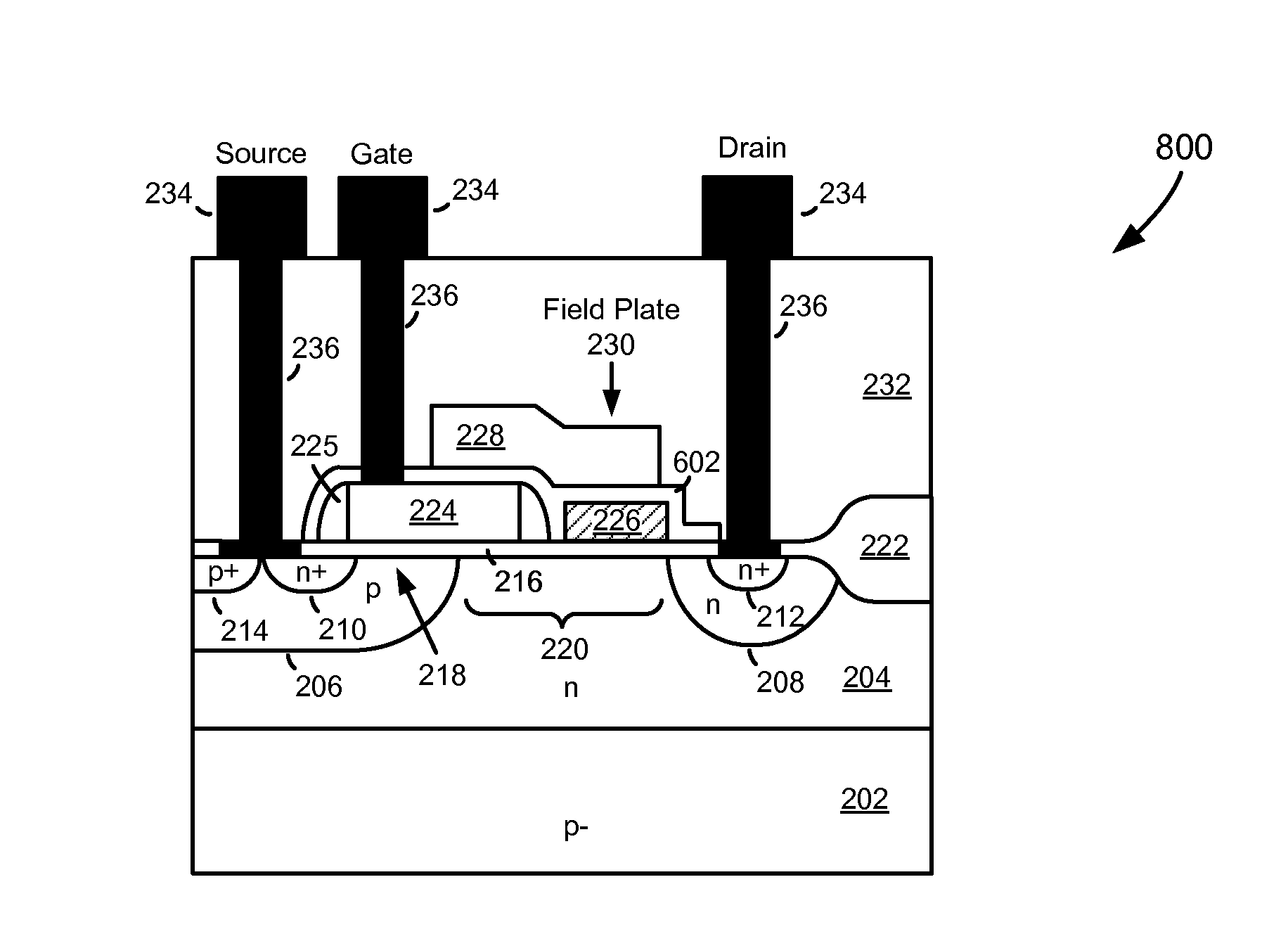
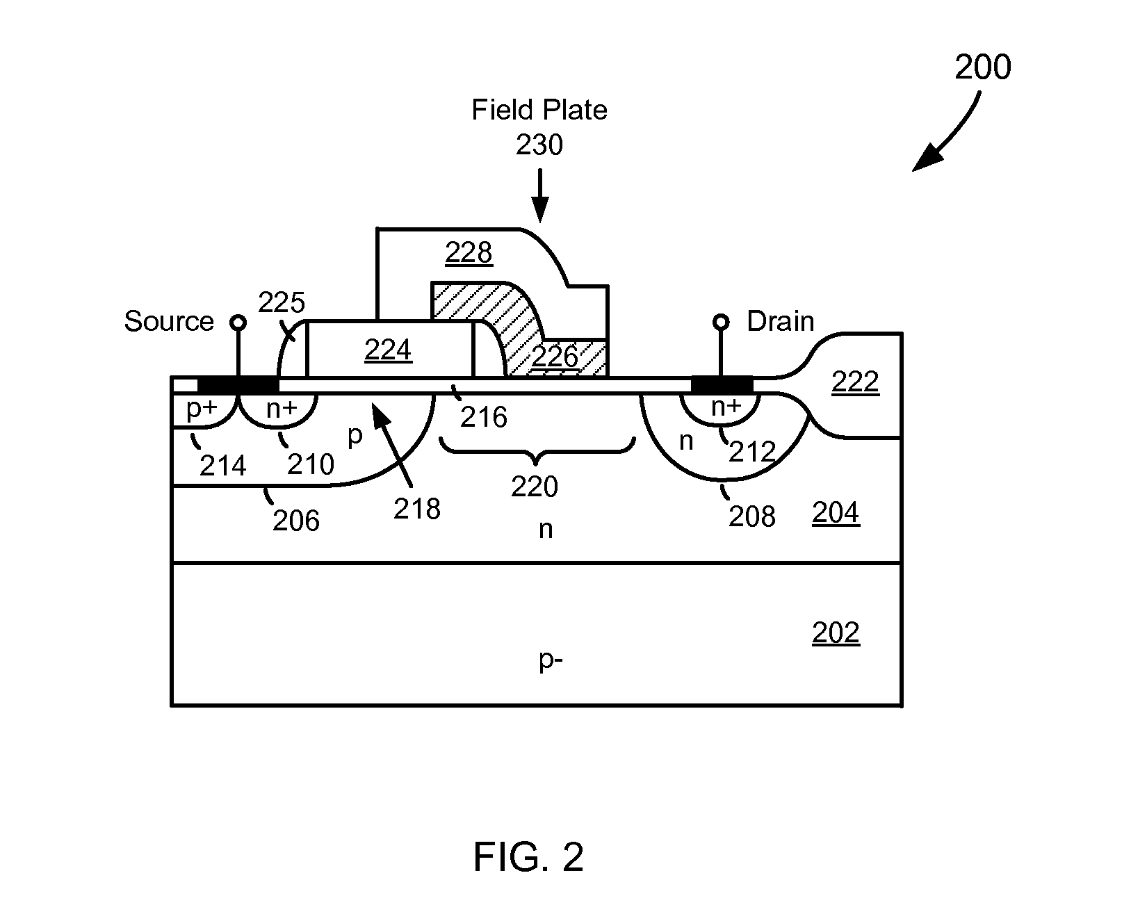
[0018]Referring to FIG. 2 there is shown a high-voltage (HV) transistor 200, according to an embodiment of the present invention. The HV transistor 200 is located in a deep n-well 204 that has been implanted and diffused in a p-type substrate 202 or, alternatively into a p-type epitaxial layer formed on a substrate. A p-body region 206 in the deep n-well 204 includes heavily-doped n+ source and p+ body contact regions 210 and 214 that are in direct electrical contact with one another. A shallow n-well 208, also formed in the deep n-well 204, contains a heavily-doped n+ drain region 212. The shallow n-well 208, which is included to reduce the on resistance (Ron) of the HV transistor 200, is separated from the p-body region 206 by a drift region 220 and has a doping concentration intermediate that of the deep n-well 204 and the n+ drain region 212. A gate dielectric layer 216 comprising silicon dioxide (SiO2) or a high-k dielectric material (“high-k” meaning a high dielectric constant...


PUM


Abstract

A high-voltage transistor is formed in a deep well of a first conductivity type that has been formed in a semiconductor substrate or epitaxial layer of a second conductivity type. A body region of the second conductivity type is formed in the deep well, into which a source region of the first conductivity type is formed. A drain region of the first conductivity type is formed in the deep well and separated from the body region by a drift region in the deep well. A gate dielectric layer is formed over the body region, and a first polysilicon layer formed over the gate dielectric layer embodies the gate of the transistor. The field plate dielectric layer is formed over the drift region after the gate has been formed. Finally, the field plate dielectric is covered by a second polysilicon layer having a field plate positioned over the field plate dielectric layer in the drift region.

Description

FIELD OF THE INVENTION[0001]The present invention is directed at high-voltage metal-oxide-semiconductor field-effect transistors and methods of their manufacture.BACKGROUND OF THE INVENTION[0002]High-voltage metal-oxide-semiconductor field-effect transistors (HV MOSFETs) are used in a wide variety of power integrated circuits (ICs). For example, they serve as high-voltage switches in high-voltage switching regulators and power management ICs. They are also used extensively in display driver ICs for modern flat panel displays. To handle the high voltages involved in these and other high-voltage applications, the HV MOSFETs must be designed to have a high breakdown voltage (BV). Further, in order to achieve high power efficiencies and realize small die sizes, the HV MOSFETs should also have low on-resistances (Ron). Unfortunately, manufacturing a HV MOSFET having both a high BV and low Ron is difficult to achieve.[0003]FIG. 1 is a cross-sectional drawing of one type of HV MOSFET, know...

Claims


Application Information

Patent Timeline
IPC IPC(8): H01L29/78H01L21/336
CPCH01L29/402H01L29/66689H01L29/7816H01L29/518H01L29/513H01L29/517H01L29/0878
Inventor JU, DONG-HYUK
Owner JU DONG HYUK
Why Eureka
Try Eureka