Light emitting element and method for manufacturing same

a technology of light-emitting elements and manufacturing methods, which is applied in the direction of lasers, semiconductor devices, semiconductor lasers, etc., can solve the problems of high power consumption, high power consumption, and power consumption reduction,

Active Publication Date: 2012-09-20
HOKKAIDO UNIVERSITY +1
View PDF12 Cites 57 Cited by
  • Summary
  • Abstract
  • Description
  • Claims
  • Application Information

AI Technical Summary

Problems solved by technology

Currently, there are two problems to be solved for the semiconductor light emitting element.
The first problem concerns the reduction of power consumption.
This problem with the semiconductor light emitting element is requires a high consumption of power, although the device lifetime is comparatively longer than that of lighting equipment that employs a filament or a fluorescent tube, this requires a high consumption of power.
The second problem concerns the provision of high luminescence.
Since, essentially, these two problems conflict with each other, these problems cannot be simultaneously solved for a conventional light emitting device having a planar p-n junction.
Furthermore, since a semiconductor nanowire has a very small diameter (width), only low-current injection is required for obtaining a radiative recombination of electron-hole pairs.

Method used


Image

  • Light emitting element and method for manufacturing same
  • Light emitting element and method for manufacturing same
  • Light emitting element and method for manufacturing same

Examples


embodiment 1

[0182]An example light emitting element of the present invention that includes an n-type silicon (111) substrate is provided for Embodiment 1.

[0183]FIG. 3 is a cross-sectional view of the structure of a light emitting element of Embodiment 1. FIG. 4 is a cross-sectional view of a core-multishell nanowire for the light emitting element of Embodiment 1 (a diagram of the cross section, perpendicular to the surface of a substrate).

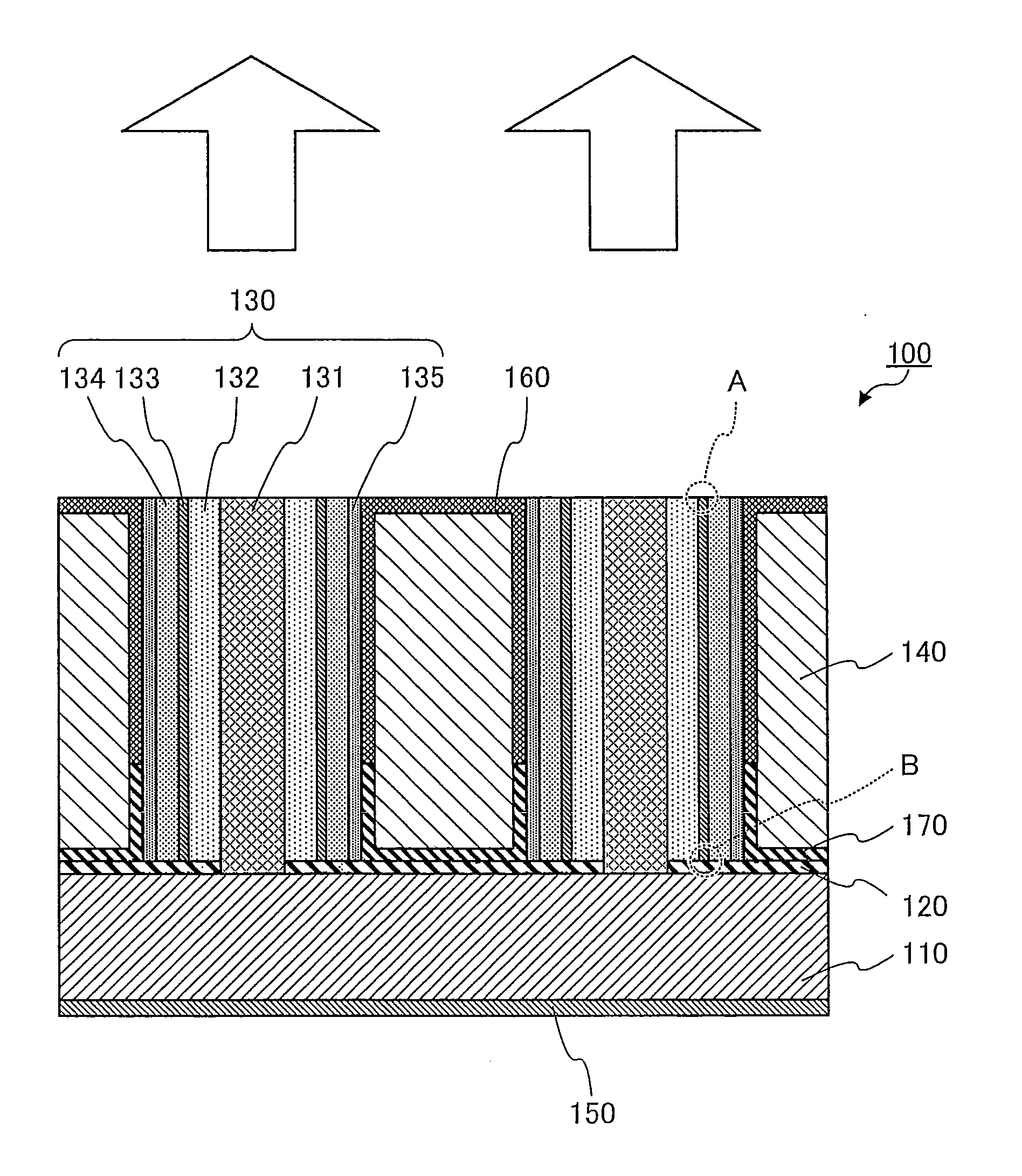
[0184]As shown in FIG. 3, a light emitting element 100 of Embodiment 1 includes an n-type silicon substrate 110, an insulating film 120, core-multishell nanowires 130, an insulating resin 140, a first electrode 150, a second electrode 160, and a dielectric film 170. As shown in FIG. 3 and FIG. 4, each of the core-multishell nanowires 130 includes: a center nanorod 131, formed of an n-type III-V compound semiconductor; a first barrier layer 132, formed of an n-type III-V compound semiconductor; a quantum well layer 133, formed of an i-type III-V compound semico...

embodiment 2

[0200]An example light emitting element for the present invention that has a p-type silicon (111) substrate is provided for Embodiment 2.

[0201]FIG. 8A is a cross-sectional view of the structure of a light emitting element for Embodiment 2. FIG. 8B is a cross-sectional view (a diagram for a cross section parallel to the surface of the substrate) of a core-multishell nanowire for the light emitting element of Embodiment 2. The same reference numerals as used for the light emitting element of Embodiment 1 are provided for the corresponding components, and an explanation for the overlapping portions will not be given.

[0202]As shown in FIG. 8A, a light emitting element 200 of Embodiment 2 includes a p-type silicon substrate 210, an insulating film 120, core-multishell nanowires 220, an insulating resin 140, a first electrode 230, a second electrode 240, and a dielectric film 170. As shown in FIG. 8A and FIG. 8B, each of the core-multishell nanowires 220 includes a center nanorod 221 form...

embodiment 3

[0209]An example light emitting element of the present invention wherein spaces between core-multishell nanowires are filled with a semi-insulating semiconductor is provided in Embodiment 3.

[0210]FIG. 9 is a cross-sectional view of the structure of a light emitting element for Embodiment 3. The same reference numerals as used for the light emitting element of Embodiment 1 are provided for the corresponding components, and an explanation for the overlapping portions will not be given.

[0211]As shown in FIG. 9, a light emitting element 300 for Embodiment 3 includes an n-type silicon substrate 110, an insulating film 120, core-multishell nanowires 130, a semi-insulating semiconductor 310, a first electrode 150, a second electrode 160, and a dielectric film 170. As shown in FIG. 9, each of the core-multishell nanowires 130 includes: a center nanorod 131, formed of an n-type III-V compound semiconductor; a first barrier layer 132, formed of an n-type III-V compound semiconductor; a quantu...


PUM


Abstract

Disclosed is a light emitting element, which emits light with small power consumption and high luminance. The light emitting element has: a IV semiconductor substrate; two or more core multi-shell nanowires disposed on the IV semiconductor substrate; a first electrode connected to the IV semiconductor substrate; and a second electrode, which covers the side surfaces of the core multi-shell nanowires, and which is connected to the side surfaces of the core multi-shell nanowires. Each of the core multi-shell nanowires has: a center nanowire composed of a first conductivity type III-V compound semiconductor; a first barrier layer composed of the first conductivity type III-V compound semiconductor; a quantum well layer composed of a III-V compound semiconductor; a second barrier layer composed of a second conductivity type III-V compound semiconductor; and a capping layer composed of a second conductivity type III-V compound semiconductor.

Description

TECHNICAL FIELD[0001]The present invention relates to a light emitting element that includes nanowires formed of III-V compound semiconductors, and to a manufacturing method therefor.BACKGROUND ART[0002]A semiconductor light emitting element, such as a light emitting diode or a semiconductor laser, has a general structure wherein an n-type semiconductor and a p-type semiconductor are junctioned together on a semiconductor substrate. Such a light emitting element emits light by employing a radiative recombination of electron-hole pairs, which occurs at a p-n junction. The semiconductor material mainly employed for the light emitting element is a III-V compound semiconductor. This is because the bandgaps (the forbidden bands) of many III-V compound semiconductors are located in the visible light region. Another reason is that, with the development of crystal growth technology in recent years, a quantum well structure, including the p-n junction of the III-V compound semiconductors, ca...

Claims


Application Information

Patent Timeline
Patent Type & Authority Applications(United States)
IPC IPC(8): H01L33/06H01L33/40B82Y99/00
CPCH01L21/02488H01S5/18369H01L21/02603H01L21/0262H01L21/02639H01L33/06H01L33/08H01L33/18H01L33/24H01L2933/0083H01S5/105H01S5/341H01S5/3428B82Y20/00H01L21/02381H01L21/02463H01S5/1042H01S5/1835H01L21/02546H01S5/11
Inventor FUKUI, TAKASHITOMIOKA, KATSUHIRO
Owner HOKKAIDO UNIVERSITY
Why Eureka
Try Eureka