Vertical hall sensor and method for producing a vertical hall sensor

a technology of vertical hall sensor and vertical hall, which is applied in the direction of galvano-magnetic device, galvano-magnetic device, instrument, etc., can solve the problems of low sensitivity, high offset, and ineffective hall voltage generation, and achieve the effect of increasing the doping and therefore the electrical conductivity below the conta

Active Publication Date: 2012-09-27
X FAB SEMICON FOUNDRIES +1
View PDF1 Cites 16 Cited by
  • Summary
  • Abstract
  • Description
  • Claims
  • Application Information

AI Technical Summary

Benefits of technology

[0019]implanting foreign atoms of the first chemical element or a third chemical element in the regions occupied by the contacts, in order to increase the doping and therefore the electrical conductivity below the contacts.

Problems solved by technology

One of the most difficult tasks in the development of the vertical Hall sensors has always been to achieve a high magnetic-field sensitivity, on the one hand, and to keep the so-called offset of the sensor signal, which is the voltage appearing between the voltage contacts in the absence of a magnetic field, as small as possible, on the other hand.
Since typical wells generated by ion implantation and subsequent relatively long diffusion have the highest doping on the surface, however, the main component of the current also flows through the Hall element just below the surface, of course, and is therefore not very effective for generating the Hall voltage, so that the sensitivity is low.
In addition, the current pathway between input current contact and output current contact is therefore very short, which has the result that even very small processing tolerances result in a high offset.

Method used


Image

  • Vertical hall sensor and method for producing a vertical hall sensor
  • Vertical hall sensor and method for producing a vertical hall sensor
  • Vertical hall sensor and method for producing a vertical hall sensor

Examples


Embodiment Construction

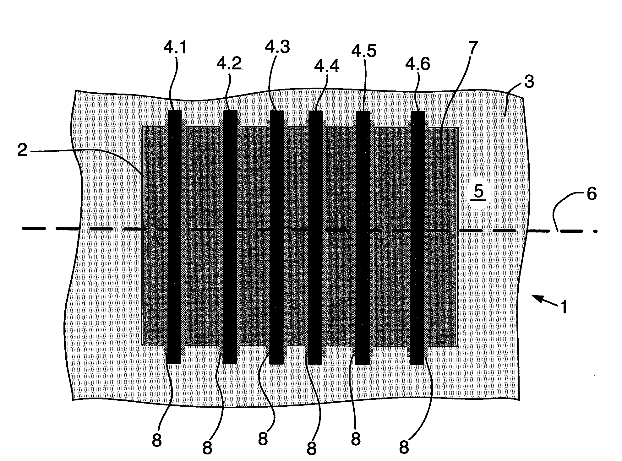
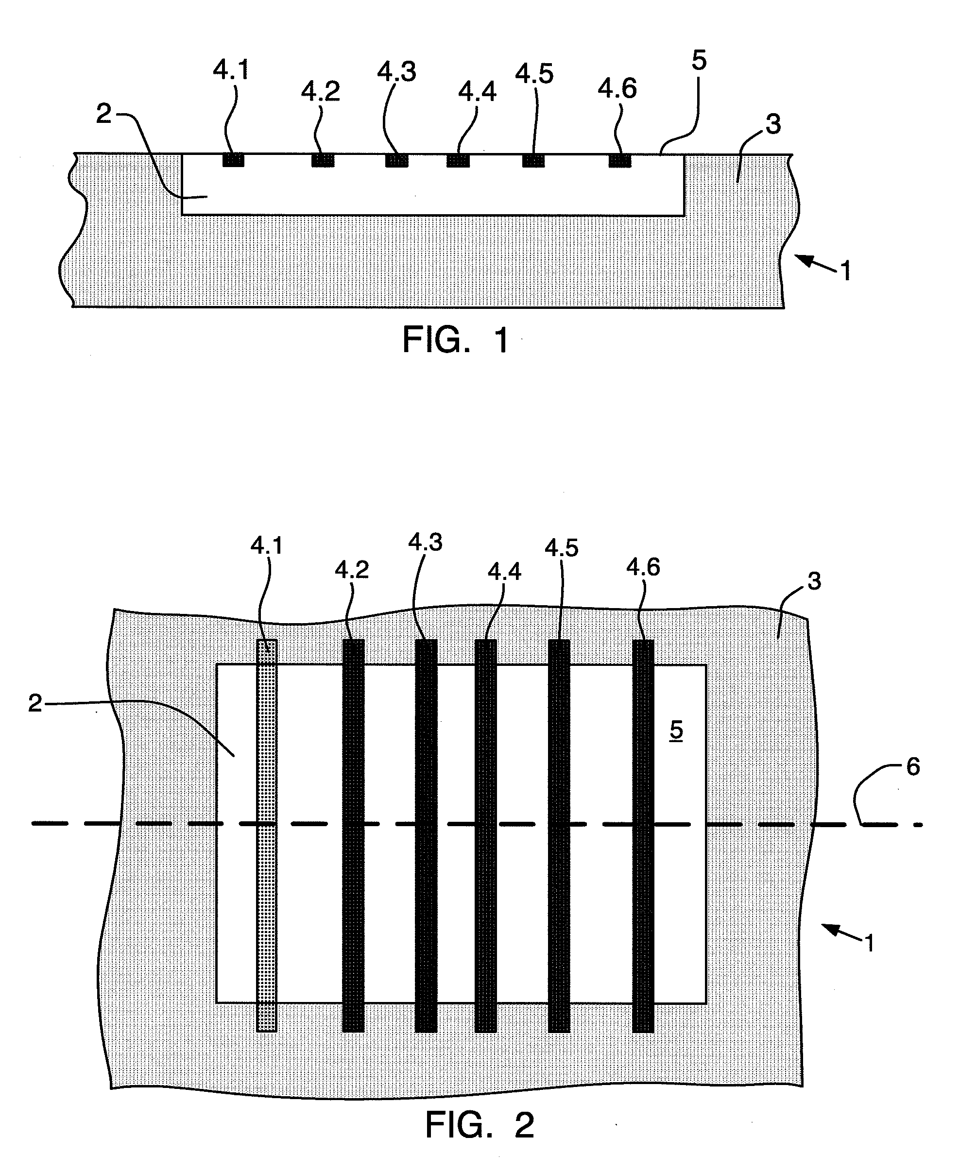
[0026]FIGS. 1 and 2 schematically show a side view and a top view of a vertical Hall sensor, which is integrated in a semiconductor chip 1. The vertical Hall sensor comprises an electrically conductive well 2 of a first conductivity type, which is embedded in an electrically conductive region 3 of a second conductivity type, and a number n of contacts 4.1 to 4.n, which contact the well 2. For the sake of simplicity, the entirety of the contacts 4.1 to 4.n is designated as the contacts 4. The contacts 4 are embedded in a surface 5 of the well 2 and arranged along a straight line 6, the surface 5 of the well 2 being located directly, i.e., only separated by typical oxidation and passivation layers, below the surface of the semiconductor chip 1, which is accessible for the wiring.

[0027]The well 2 preferably comprises n-doped semiconductor material and the region 3 comprises p-doped semiconductor material. The well 2 is therefore electrically insulated from the region 3 by a pn-junction...


PUM


Abstract

The invention relates to a vertical Hall sensor integrated in a semiconductor chip and a method for the production thereof. The vertical Hall sensor has an electrically conductive well of a first conductivity type, which is embedded in an electrically conductive region of a second conductivity type. The electrical contacts are arranged along a straight line on a planar surface of the electrically conductive well. The electrically conductive well is generated by means of high-energy ion implantation and subsequent heating, so that it has a doping profile which either has a maximum which is located at a depth T1 from the planar surface of the electrically conductive well, or is essentially constant up to a depth T2.

Description

[0001]PRIORITY CLAIM[0002]Applicant hereby claims foreign priority under 35 U.S.C §119 from Swiss Application No. 531 / 11 filed Mar. 24, 2011, the disclosure of which is herein incorporated by reference.FIELD OF THE INVENTION[0003]The invention relates to a vertical Hall sensor, which is integrated in a semiconductor chip, and a method for producing such a vertical Hall sensor.BACKGROUND OF THE INVENTION[0004]A vertical Hall sensor is a magnetic field sensor which is sensitive to a magnetic field which extends parallel to the surface of the semiconductor chip. The vertical Hall sensor typically comprises an n-doped well, which has been diffused into a p-doped substrate, or a p-doped well, which has been diffused into an n-doped substrate, the well typically having four or five contacts, which are arranged along a straight line and are located on the surface of the semiconductor chip. Two or three of the four contacts are current contacts which are used for the purpose of causing a cu...

Claims


Application Information

Patent Timeline
Patent Type & Authority Applications(United States)
IPC IPC(8): H01L43/06H01L43/14
CPCG01R33/077H01L43/14H01L43/065H10N52/101H10N52/01G01R33/07
Inventor SCHOTT, CHRISTIANHOFMANN, PETER
Owner X FAB SEMICON FOUNDRIES
Why Eureka
Try Eureka