Dual gate oxide high-voltage semiconductor device and method for forming the same

a high-voltage semiconductor and gate oxide technology, applied in the direction of semiconductor devices, electrical devices, transistors, etc., can solve the problems of reducing affecting the performance of the device, so as to reduce the specific-on-resistance of the device and increase the doping in the silicon layer drift region.

Inactive Publication Date: 2005-04-21
NXP BV
View PDF5 Cites 2 Cited by
  • Summary
  • Abstract
  • Description
  • Claims
  • Application Information

AI Technical Summary

Benefits of technology

[0008] The present invention overcomes the drawbacks associated with other devices by providing a dual gate high-voltage semiconductor device. The dual gate oxide of the present invention allows the figures of merit for a high-voltage device (i.e., breakdown voltage and specific-on-resistance) to be improved. Specifically, the device of the present invention includes a semiconductor substrate, a buried oxide layer over the substrate, a silicon layer over the buried oxide layer, a first gate oxide over the silicon layer adjacent a top oxide layer, and a second gate oxide over the first gate oxide. By forming the second gate oxide, the doping in the drift region of the silicon layer can be increased without increasing the magnitude of the vertical electric field. This allows the specific-on-resistance of the device to be reduced without degrading the breakdown voltage.

Problems solved by technology

In fabricating high-voltage power devices, tradeoffs and compromises must often be made in areas such as breakdown voltage, specific-on resistance, size, conduction losses, manufacturing simplicity, and reliability.
Frequently improvement of one characteristic such as breakdown voltage can lead to degradation in another such as specific-on-resistance.
However, an increase in doping causes an increase in a magnitude of the electric field, which degrades the breakdown voltage of the device.
This often leads to bottlenecking for current flow, and preventing optimum reduction in conduction losses.

Method used


Image

  • Dual gate oxide high-voltage semiconductor device and method for forming the same
  • Dual gate oxide high-voltage semiconductor device and method for forming the same
  • Dual gate oxide high-voltage semiconductor device and method for forming the same

Examples


Embodiment Construction

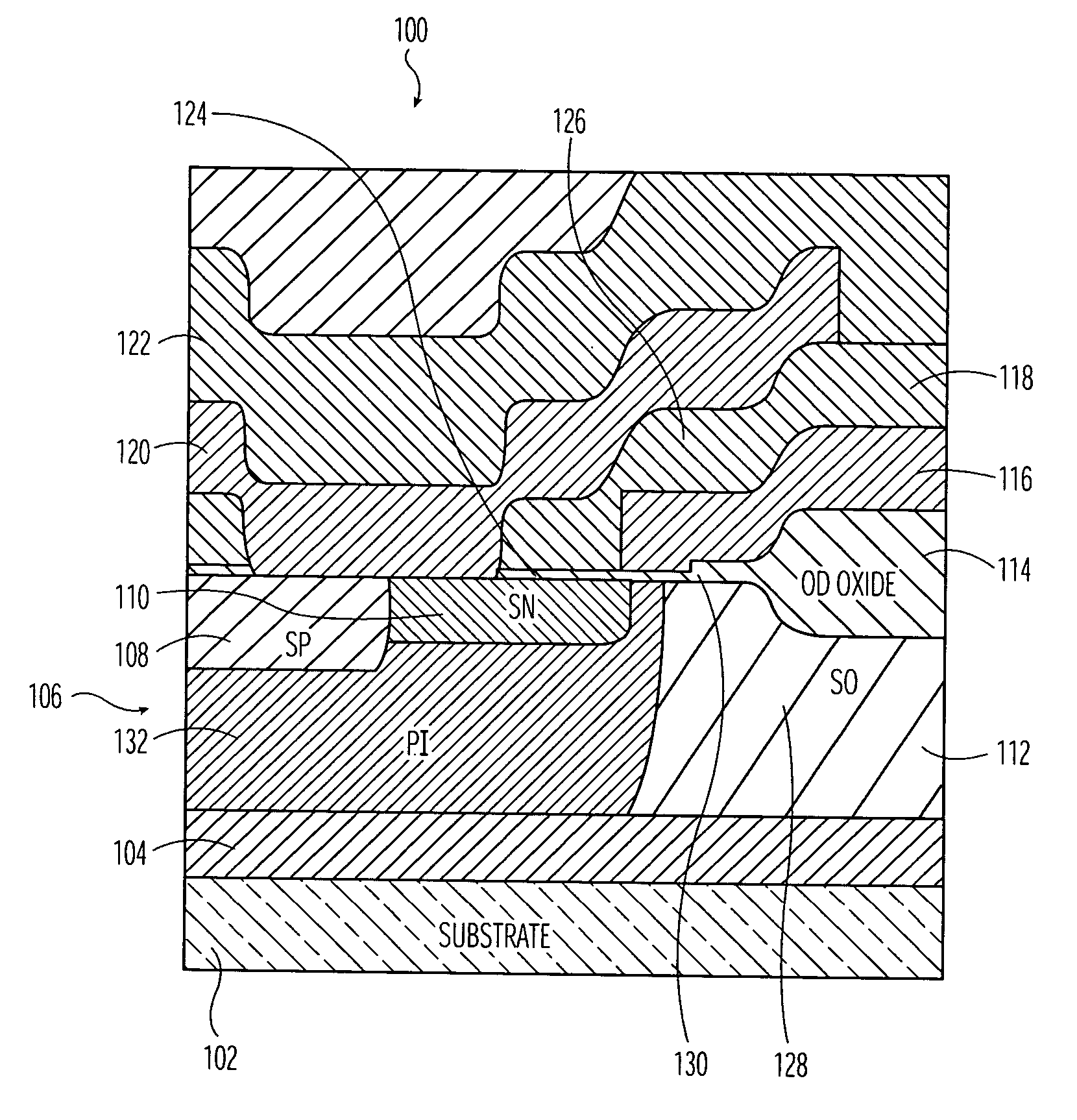
[0018] In general, the present invention provides a dual gate oxide high-voltage semiconductor device. Specifically, a high-voltage device, such as a lateral MOSFET, constructed according to the present invention is provided with a dual gate oxide so that the breakdown voltage can be increased while the specific-on-resistance of the device can be decreased.

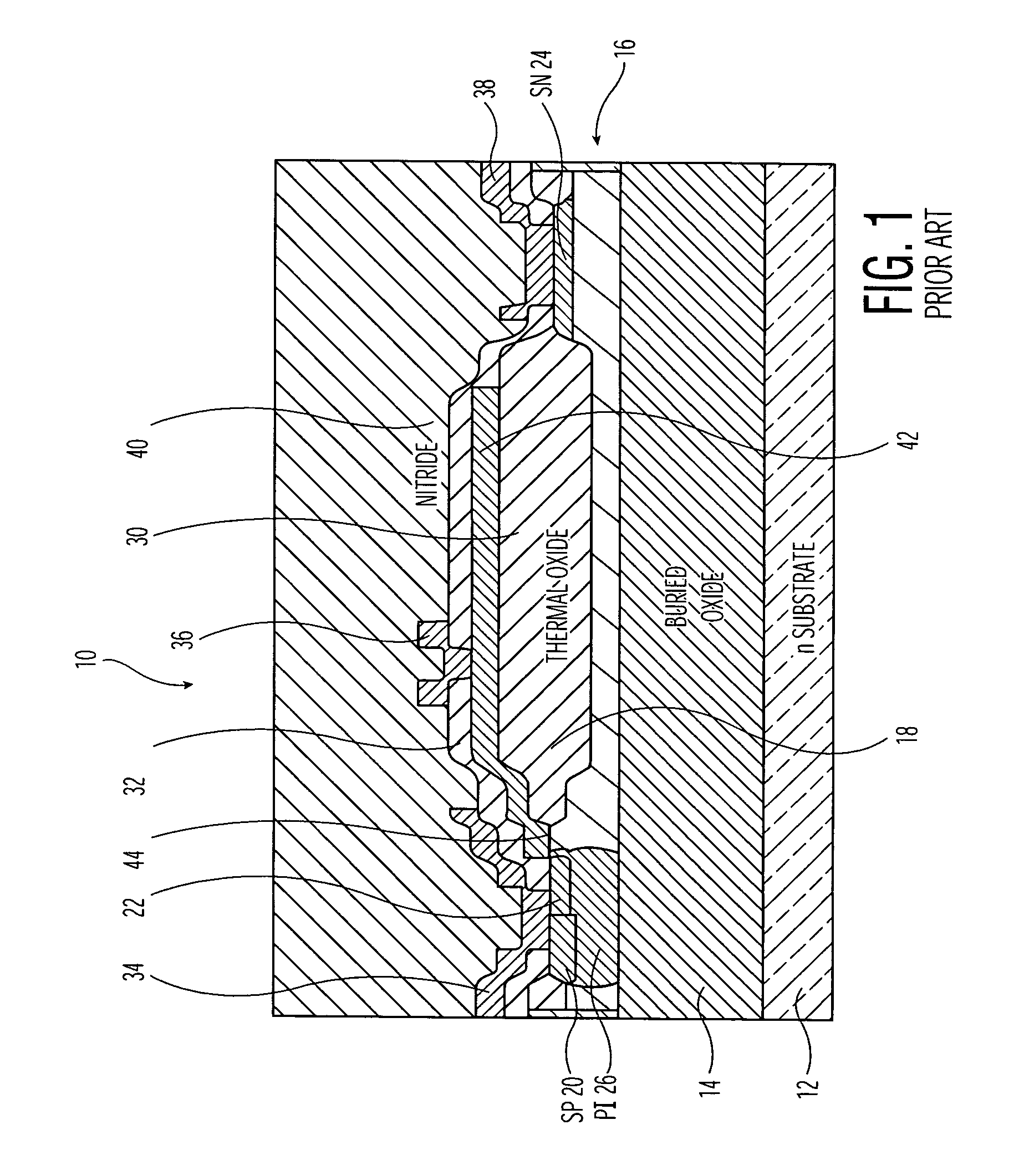
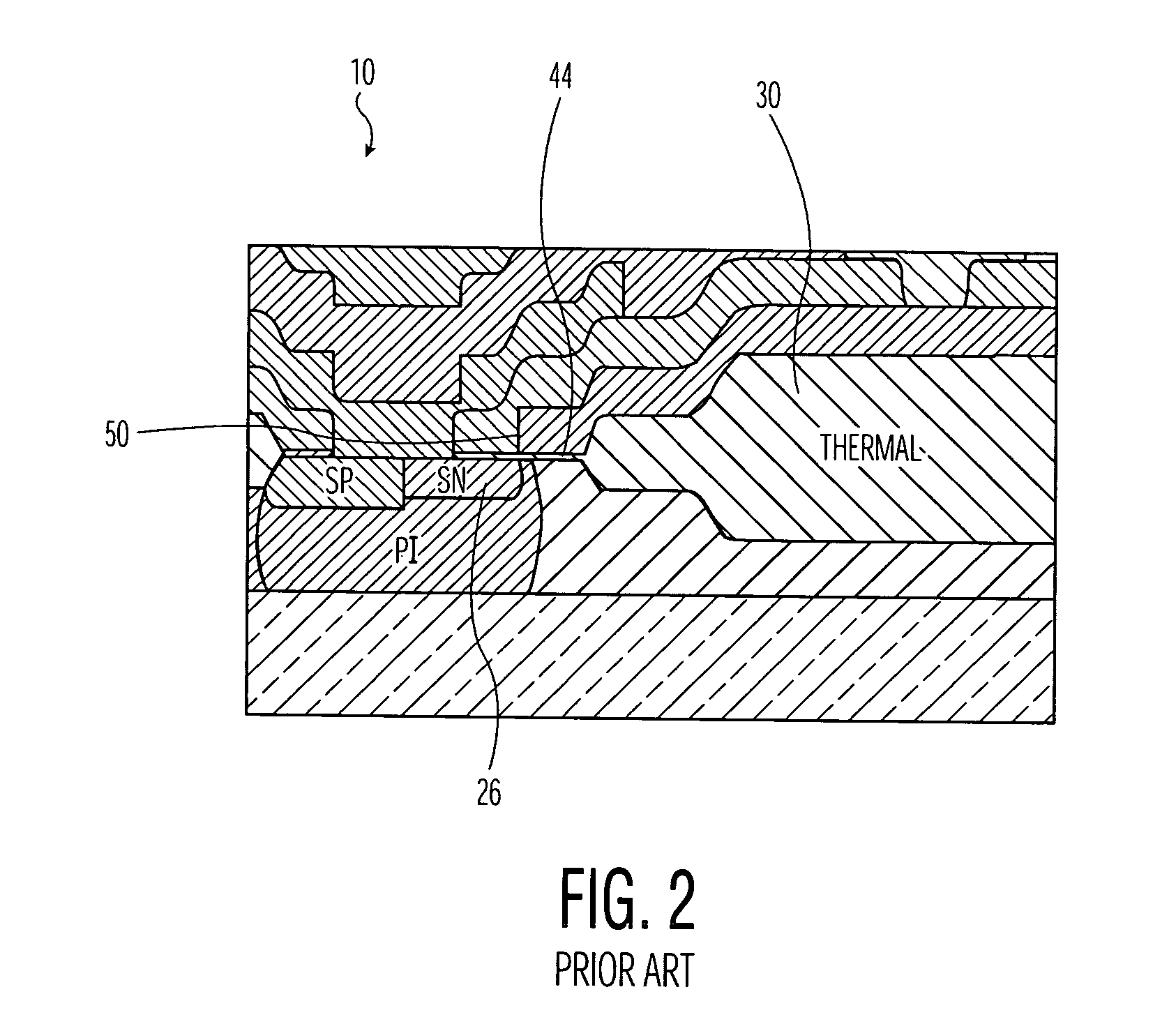
[0019] Referring now to FIG. 1, a related art high-voltage semiconductor device 10 is shown. As shown, silicon (SOI) layer 16 is formed over silicon substrate 12 with buried oxide layer 14 interposed therebetween. Silicon layer 16 is doped as known in the art by providing a mask (e.g., a patterned photoresist layer) on silicon layer 16 and implanting ions, as described in detail in U.S. Pat. No. 5,300,448. Top or thermal oxide layer 30 is formed using a standard Local Oxidation of Silicon (LOCOS) technique. This involves growing a pad oxide layer on silicon layer 16 and then depositing a silicon nitride layer on the pad oxide lay...


PUM


Abstract

A dual gate oxide high-voltage semiconductor device and method for forming the same are provided. Specifically, a device formed according to the present invention includes a semiconductor substrate, a buried oxide layer formed over the substrate, a silicon layer formed over the buried oxide layer, and a top oxide layer formed over the silicon layer. Adjacent an edge of the top oxide layer, a dual gate oxide is formed. The dual gate oxide allows both specific-on-resistance and breakdown voltage of the device to be optimized.

Description

BACKGROUND OF THE INVENTION [0001] 1. Field of the Invention [0002] The present invention generally relates to a dual gate oxide high-voltage semiconductor (SOI) device. More particularly, the present invention relates to a high-voltage semiconductor device, such as a lateral MOSFET or a diode, having two gate oxides for optimizing breakdown voltage and specific-on-resistance. [0003] 2. Background Art [0004] In fabricating high-voltage power devices, tradeoffs and compromises must often be made in areas such as breakdown voltage, specific-on resistance, size, conduction losses, manufacturing simplicity, and reliability. Frequently improvement of one characteristic such as breakdown voltage can lead to degradation in another such as specific-on-resistance. For example, to reduce the specific-on-resistance of a device, silicon doping is often increased. However, an increase in doping causes an increase in a magnitude of the electric field, which degrades the breakdown voltage of the d...

Claims


Application Information

Patent Timeline
Patent Type & Authority Applications(United States)
IPC IPC(8): H01L21/28H01L29/786H01L29/423H01L29/78
CPCH01L21/28247H01L29/7824H01L29/42368H01L21/18H01L27/08
Inventor LETAVIC, THEODORE J.SIMPSON, MARK R.
Owner NXP BV
Why Eureka
Try Eureka