Planar broadband traveling-wave beam-scan array antennas

a beam-scan array and broadband technology, applied in the field of radiofrequency antennas, can solve the problems of unsuitable application applications, disruptive effects, and unfavorable many low-cost production techniques, and achieve the effect of improving specific performan

Active Publication Date: 2012-10-04
WANG ELECTRO OPTO
View PDF0 Cites 19 Cited by
  • Summary
  • Abstract
  • Description
  • Claims
  • Application Information

AI Technical Summary

Benefits of technology

[0015]One or more layers of dielectric or magneto-dielectric substrates can be placed between the planar TW antenna elements and the ground plane, or as superstrate placed above the TW antenna elements, or both, for enhancement of specific performances.

Problems solved by technology

3-D elements have a large dimension perpendicular to the plane of the array (along the z axis), thus are not amenable to many low-cost production techniques.
The resulting bidirectional radiation renders this planar array unsuitable for applications in which conformal mounting on a platform is required.
When Hansen added a ground plane to one side of array to suppress its back radiation, he noted disruptive effects.
Therefore, Hansen's array is impractical, just like Wheeler's array, until a ground plane is added.
Claiming a wide operating bandwidth much more than 10:1, the FA approach has insufficient supporting data in the open literature.
Indeed, as observed by Thors et al (2005), design guidelines and results are often scant or nonexistent in the documents on CSA and FA.
It must be emphasized that, even though extremely broad bandwidth can be easily designed for the case of planar arrays of 2-D elements with no supporting ground plane, design of broadband planar array having a ground plane is difficult.
This inventor noted that the theory and experimentation on CSA and FA disclosed to the public often are indirect and incomplete, and have not yet realized full-fledged broadband performance as claimed.
He also noted some limitations and deficiencies in certain design concepts of CSA and FA, which consist of inherently narrowband components whose bandwidths are difficult to broaden by reconfiguration or optimization.

Method used


Image

  • Planar broadband traveling-wave beam-scan array antennas
  • Planar broadband traveling-wave beam-scan array antennas
  • Planar broadband traveling-wave beam-scan array antennas

Examples


experimental verification

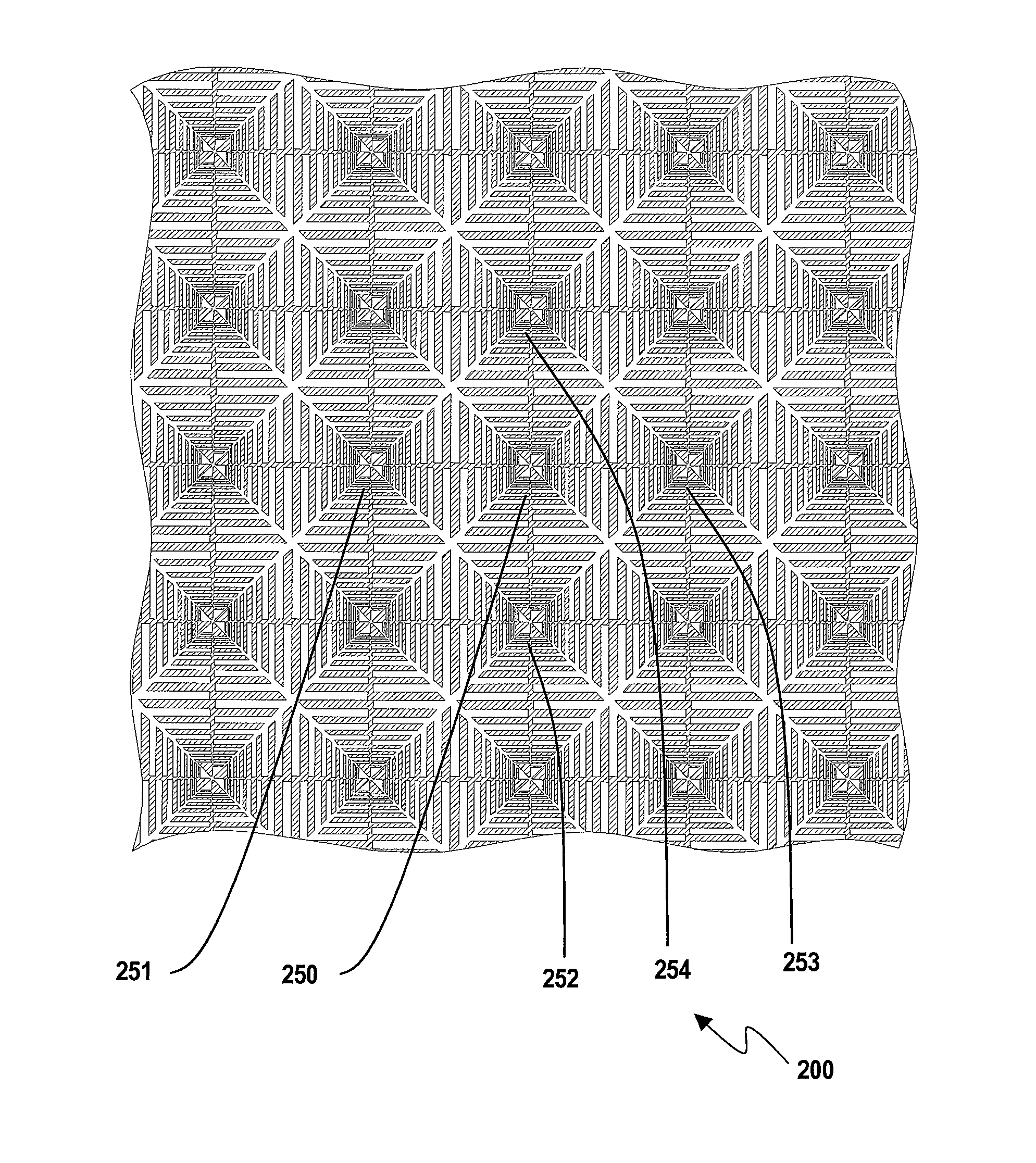
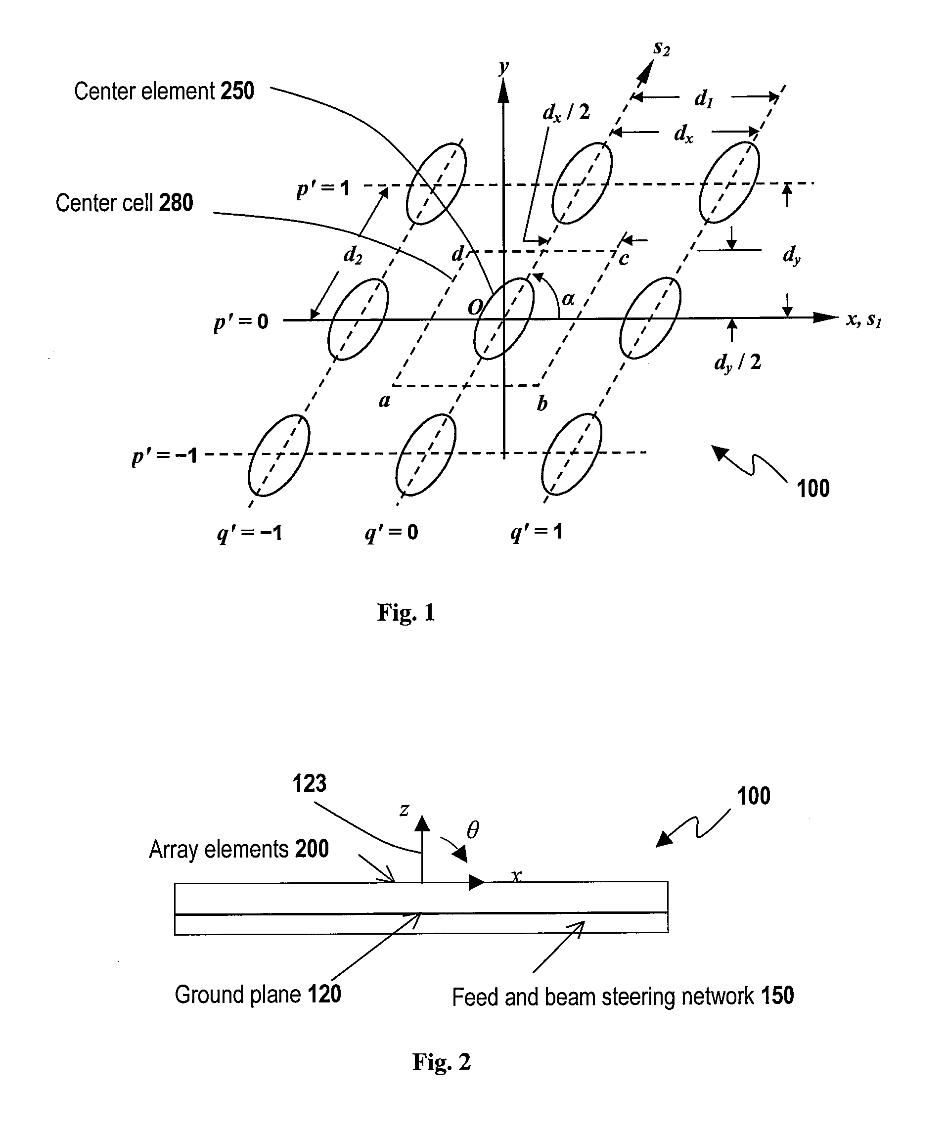
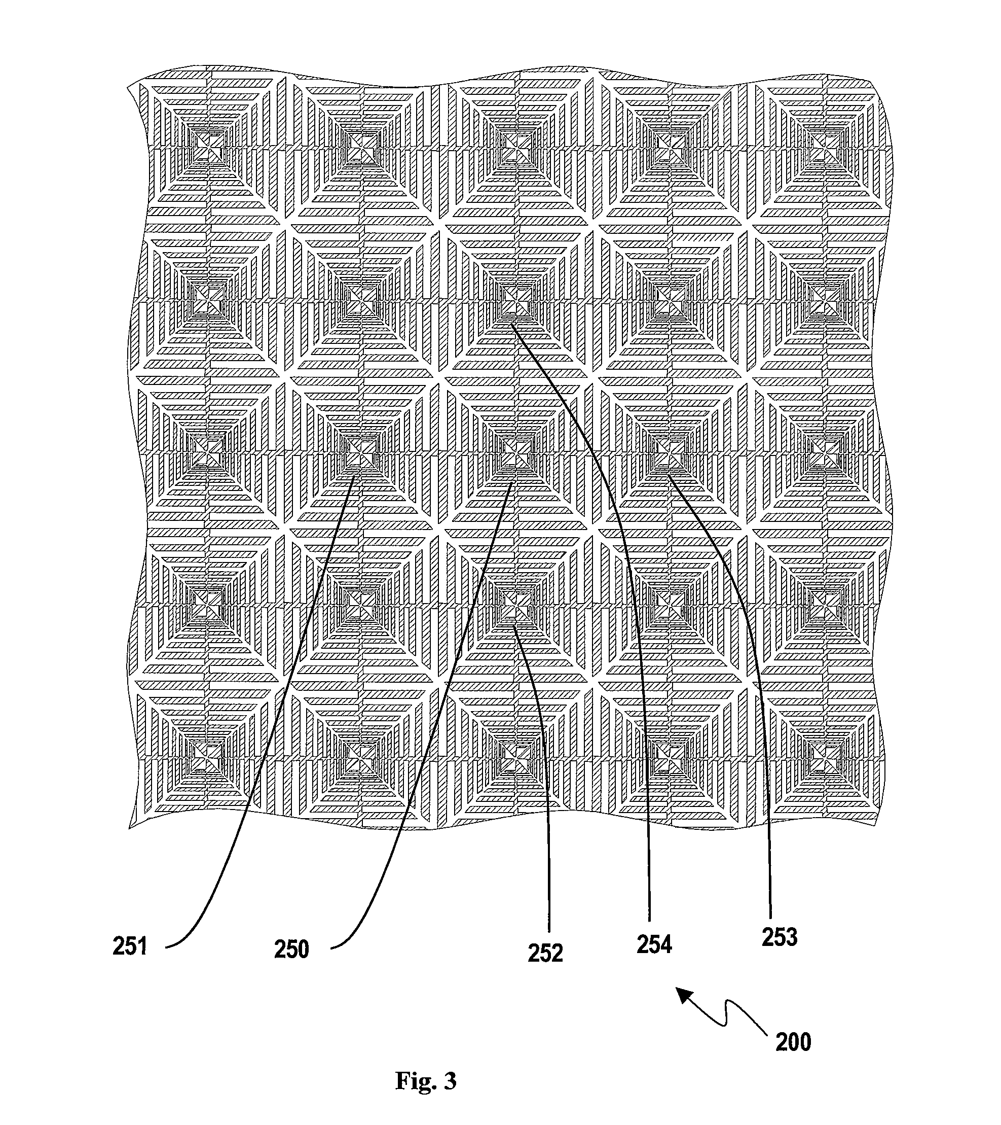
[0051]Basic experimentation has been performed for this invention. A breadboard 5×5-cell planar array similar to that in FIGS. 3-5 was designed, fabricated, and tested. Each cell has both x and y directed LP planar dipoles. The vertical center element has a broadband balun feed across its feed terminals (corresponding to 250b and 250d in FIG. 5). Each of the other 24 vertical LP dipoles has a 100-ohm resistor load. All the 25 horizontal LP dipoles have their feed terminals (corresponding to 250a and 250c in FIG. 5) floating (open-circuit with no connection to other element or device).

[0052]According to the theory and practices in planar arrays, the properties of a large planar array can be determined by measuring its “active element gain pattern,” which takes account of the mutual coupling and beam scan of a planar array (Mailloux, 1994; Pozar, 1994). The active gain pattern reveals the scan property of the element antenna, including both impedance matching and radiation pattern. Th...


PUM


Abstract

A planar broadband beam-steering phased array antenna with approximately 10:1 bandwidth is comprised of planar broadband traveling wave antenna elements positioned parallel to a conducting ground plane and spaced less than 0.5 wavelength at the highest operating frequency and more than 0.01 wavelengths at the lowest operating frequency. Each planar traveling wave antenna element is a planar frequency-independent antenna or planar self-complementary antenna, and is truncated to fit a unit cell of the phased array. Adjacent antenna elements are arranged to be tightly coupled together or connected with each other and spaced less than 0.5 wavelength apart between their centers throughout its operating frequency range. One or more layers of dielectric or magneto-dielectric substrates / superstrates can be added to enhance specific performances.

Description

TECHNICAL FIELD[0001]The present invention is generally related to radio-frequency antennas and, more particularly, broadband planar beam-scan array antennas.BACKGROUND OF THE INVENTION[0002]Broadband planar array antennas have become increasingly more important for both military and commercial applications. The broadband requirement is driven by the proliferation of wireless systems operating at different separate frequencies and the need for high speed. The planar form factor is desirable and often necessary for both transport and installation of the array antenna, because of the associated features of low profile and conformability to platform. The planar form also lends itself to low weight and low-cost production methods such as a printed-circuit board.[0003]The planar array antenna consists of identical and generally equally-spaced element antennas periodically positioned on a planar surface (the x-y plane) of the array antenna, as depicted in FIG. 1. The periodicity is along ...

Claims


Application Information

Patent Timeline
Patent Type & Authority Applications(United States)
IPC IPC(8): H01Q9/04H01Q5/00
CPCH01Q1/38H01Q3/26H01Q21/0037H01Q13/206H01Q11/04
Inventor WANG, JOHNSON J. H.
Owner WANG ELECTRO OPTO
Why Eureka
Try Eureka