

Plasma-nitriding method
- Summary
- Abstract
- Description
- Claims
- Application Information
AI Technical Summary
Benefits of technology
Problems solved by technology
Method used
Image

Examples
first embodiment
[0018]Hereinafter, a first embodiment of the present invention will be described with reference to the accompanying drawings which form a part hereof. A plasma-nitriding method of this embodiment includes performing a plasma-nitriding process on a target object in a processing chamber of a plasma processing apparatus by using a plasma of a processing gas containing a nitrogen-containing gas and a rare gas, the target object having a silicon nitride film formed by an ALD method.
Plasma Processing Apparatus
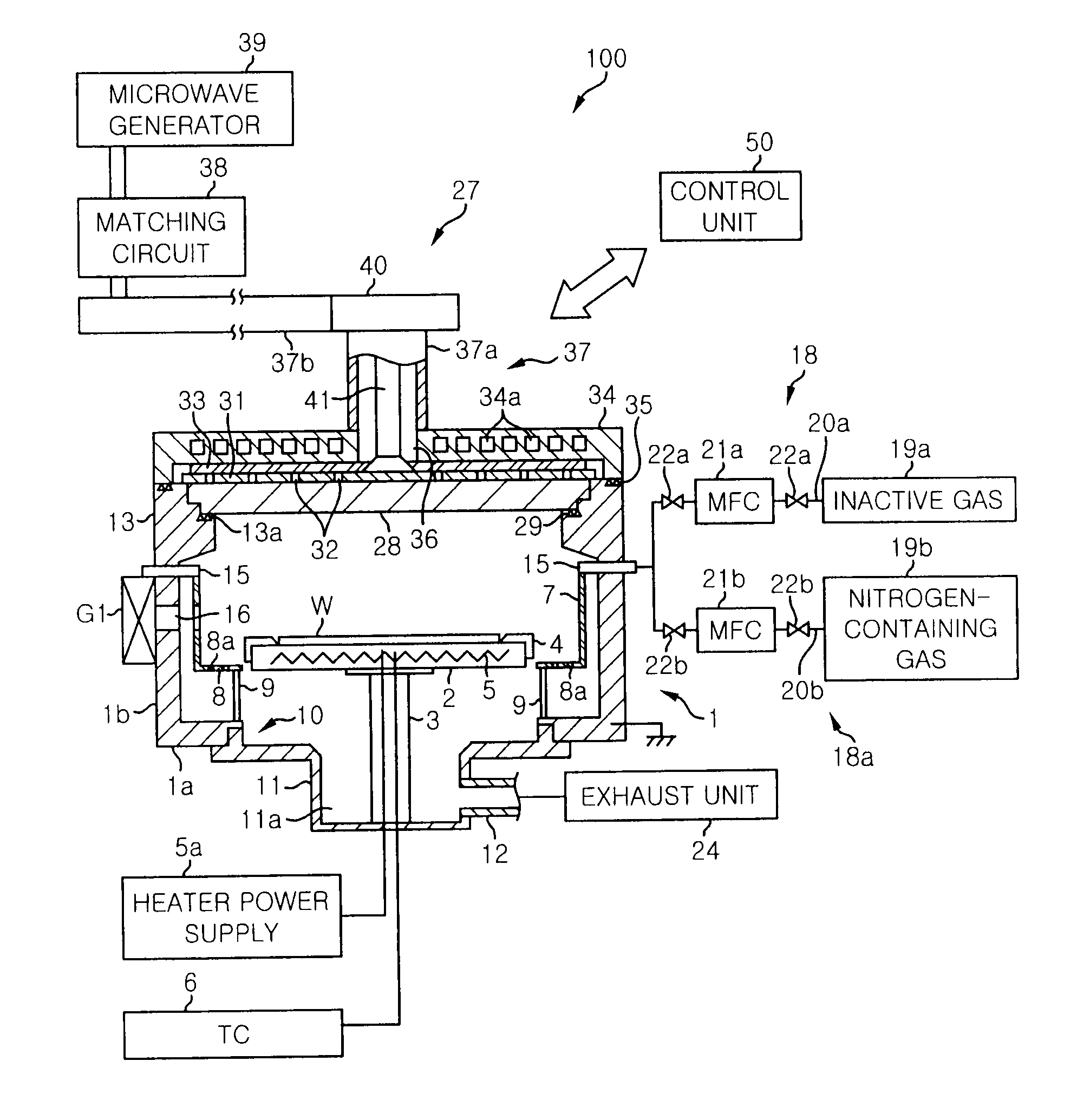
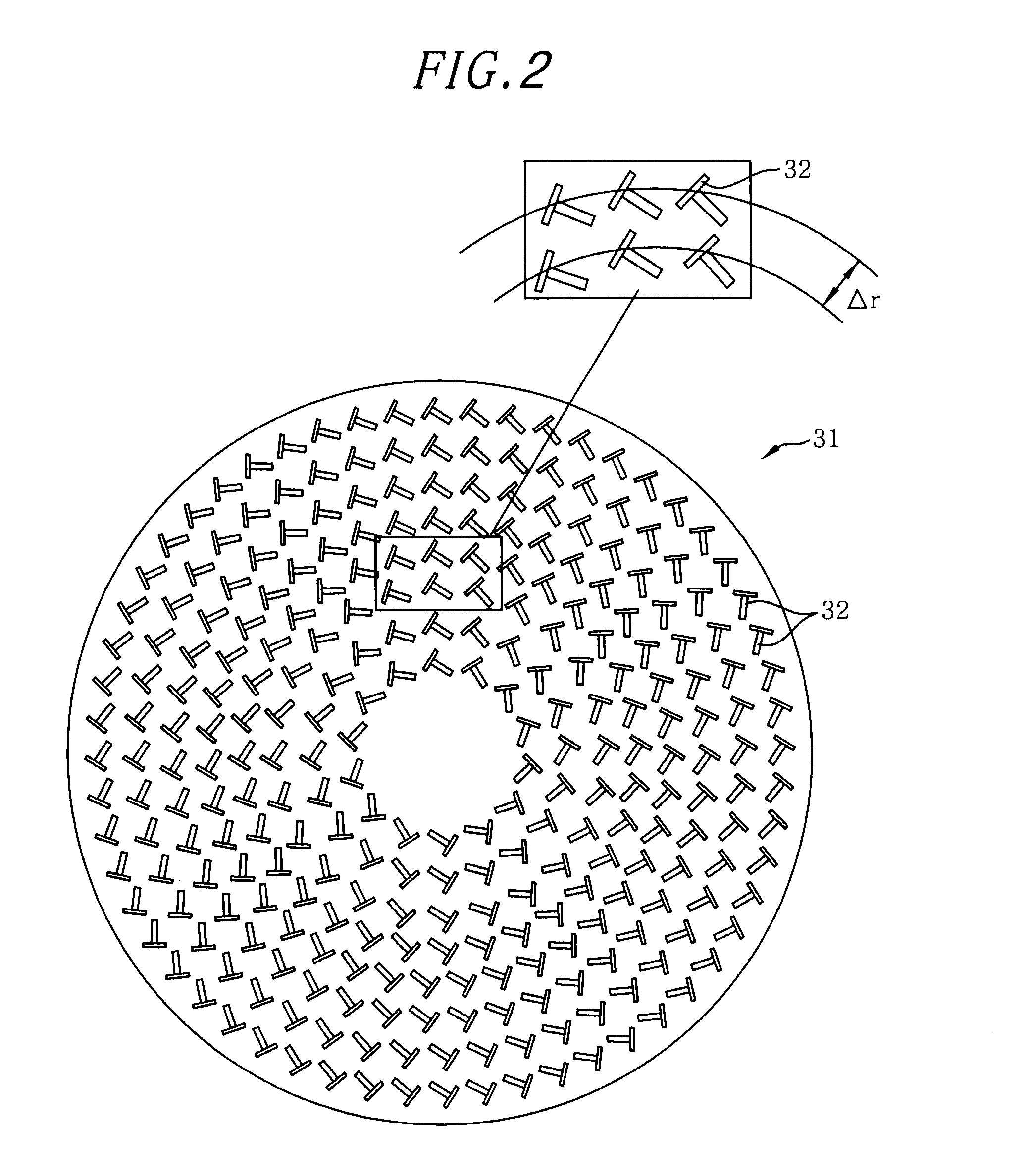
[0019]First, a plasma processing apparatus that can be used preferably in the plasma-nitriding method of this embodiment will be described with reference to FIGS. 1 to 3. FIG. 1 is a cross-sectional view schematically showing a configuration of a plasma processing apparatus 100 used in the plasma-nitriding method of this embodiment. FIG. 2 is a plan view showing a planar antenna of the plasma processing apparatus 100 shown in FIG. 1. FIG. 3 shows a configuration example of a control ...
second embodiment
[0131]In the first embodiment, mainly, modification of the
[0132]SiN film used as a spacer film, a liner film, a sidewall film, a cap film or the like of a semiconductor device has been described as an example. However, the plasma-nitriding method of the present invention may be applied for other purposes. For example, when a device isolation film is formed by shallow trench isolation (STI), after a SiN film is formed on an inner surface of a silicon trench by the ALD method, a SiO2 film may be embedded as a device isolation film in the trench. In this case, oxygen in the embedded SiO2 film reaches an interface between the SiN film and silicon through the SiN film, and reacts with silicon to form SiO2. The SiN film is converted into a SiON film to substantially grow the film.
[0133]As a result, a device formation region becomes small, and it is impossible to stably manufacture a device, thereby reducing a yield. In order to avoid such problems, the plasma-nitriding process may be perf...
PUM
| Property | Measurement | Unit |
|---|---|---|
| Temperature | aaaaa | aaaaa |
| Temperature | aaaaa | aaaaa |
| Fraction | aaaaa | aaaaa |
Abstract
Description
Claims
Application Information