Process for damascene structure with reduced low-k damage

a damascene and low-k-damage technology, applied in the field of damascene structure processing, can solve the problems of complex integrated circuits, degrade the overall performance of integrated circuits, and delay in capacitance (rc), so as to prevent copper migration into surrounding layers, improve electrical properties of circuit devices, and enhance copper passivation

Active Publication Date: 2012-10-04
APPLIED MATERIALS INC
View PDF6 Cites 24 Cited by
  • Summary
  • Abstract
  • Description
  • Claims
  • Application Information

AI Technical Summary

Benefits of technology

[0009]In one embodiment, the method for forming a semiconductor structure comprising depositing a sacrificial dielectric material over a dielectric base layer, forming a damascene feature into the sacrificial dielectric material and the dielectric base layer, filling the damascene feature with a conductive material, removing the sacrificial dielectric material located trench areas between the filled damascene feature, and filling the trench areas with a low-k dielectric material. In one aspect, the method further includes selectively depositing a passivating layer made of cobalt or a cobalt alloy on a top surface of the conductive material. In another aspect, before removing the sacrific

Problems solved by technology

Integrated circuits have evolved into complex devices that can include millions of components (e.g., transistors, capacitors and resistors) on a single chip.
At sub-micron dimensions, capacitive coupling potentially occurs between adjacent metal interconnects, which may cause cross talk and/or resistance-capacitance (RC) delay and degrade the overall performance of the int

Method used


Image

  • Process for damascene structure with reduced low-k damage
  • Process for damascene structure with reduced low-k damage
  • Process for damascene structure with reduced low-k damage

Examples


Embodiment Construction

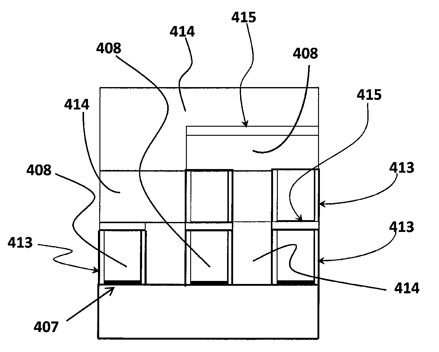
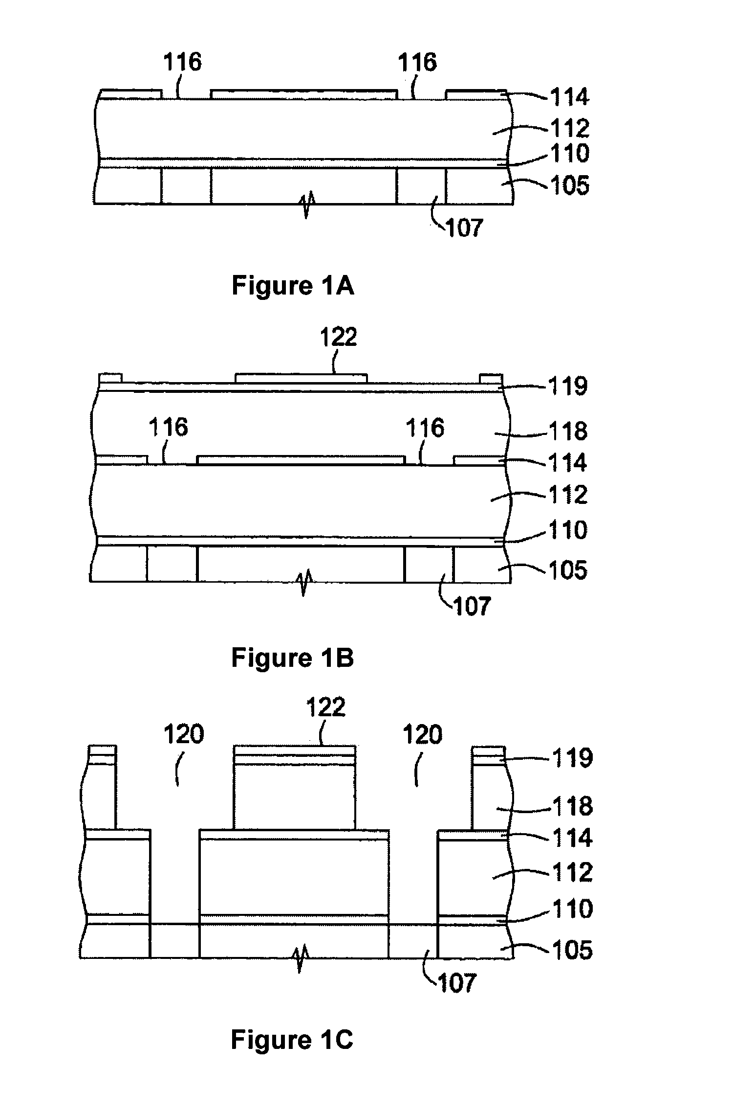
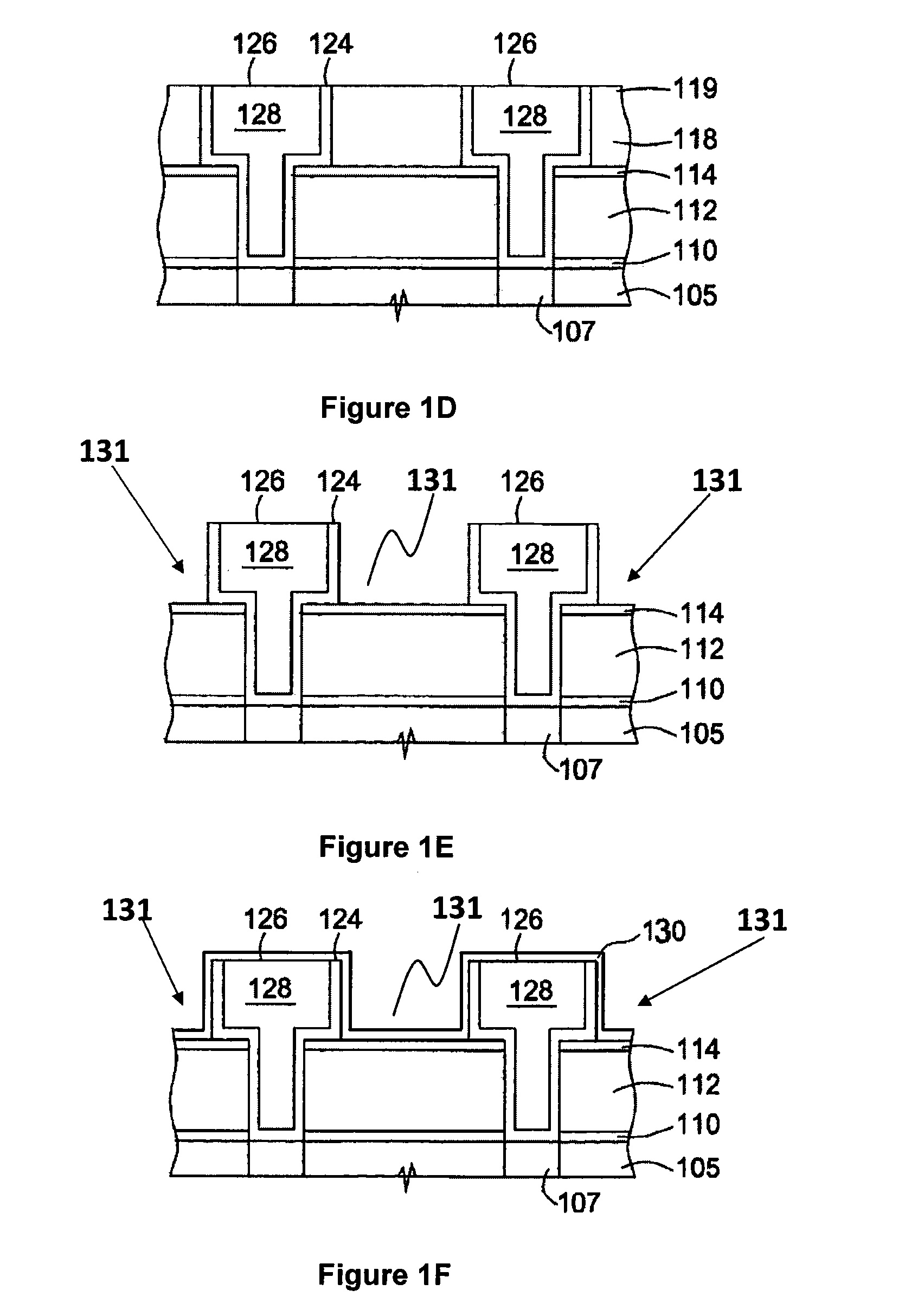
[0016]Embodiments described herein generally provide methods for reducing undesired low-k damages during a damascene process using a sacrificial dielectric material and optionally a barrier / capping layer. In various embodiments, a damascene structure is formed through a sacrificial dielectric material deposited over a preexisting base layer, which may be one or more dielectric materials such as doped or undoped silicon oxides having conductive features formed therein. The damascene structure is filled with a suitable metal such as copper. The sacrificial dielectric material filled in trench areas between the copper damascene is then removed, followed by various barrier / cap schemes conformally or selectively covering exposed surfaces of the copper damascene structure. Thereafter, ultra low-k dielectric materials may fill the trench areas that were previously filled with sacrificial dielectric material. The process may be repeated as necessary with any desired pattern and etch process...


PUM


Abstract

Embodiments described herein generally provide methods for reducing undesired low-k damages during a damascene process using a sacrificial dielectric material and optionally a barrier/capping layer. In one embodiment, a damascene structure is formed through a sacrificial dielectric material deposited over a dielectric base layer. The damascene structure is filled with a suitable metal such as copper. The sacrificial dielectric material filled in trench areas between the copper damascene is then removed, followed by a barrier/cap layer which conformally or selectively covers exposed surfaces of the copper damascene structure. Ultra low-k dielectric materials may then fill the trench areas that were previously filled with sacrificial dielectric material. The invention prevents the ultra low-k material between the metal lines from exposing to various damaging processes during a damascene process such as etching, stripping, wet cleaning, pre-metal cleaning or CMP process.

Description

CROSS-REFERENCE TO RELATED APPLICATIONS[0001]This application claims benefit of U.S. provisional patent application Ser. No. 61 / 470,386, filed Mar. 31, 2011, entitled “PROCESS FOR DAMASCENE STRUCTURE WITH REDUCED LOW-K DAMAGE”, which is herein incorporated by reference.BACKGROUND OF THE INVENTION[0002]1. Field of the Invention[0003]Embodiments of the present invention generally relates to semiconductor processing technologies and, more specifically, to improved methods for fabricating a damascene structure without damaging low-k dielectric materials in the structure.[0004]2. Description of the Related Art[0005]Integrated circuits have evolved into complex devices that can include millions of components (e.g., transistors, capacitors and resistors) on a single chip. The demand for greater circuit density necessitates a reduction in the dimensions of the integrated circuit components, e.g., sub-micron dimensions and the use of various materials to fabricate devices in order to achieve...

Claims


Application Information

Patent Timeline
IPC IPC(8): H01L21/768
CPCH01L21/76885H01L21/7681H01L21/76834H01L21/02697H01L21/76856H01L21/76873H01L21/7685H01L29/66583H01L21/28H01L21/768
Inventor NAIK, MEHUL B.CUI, ZHENJIANG
Owner APPLIED MATERIALS INC
Why Eureka
Try Eureka