Oxide semiconductor film and semiconductor device

Active Publication Date: 2012-10-18
SEMICON ENERGY LAB CO LTD
View PDF19 Cites 43 Cited by
  • Summary
  • Abstract
  • Description
  • Claims
  • Application Information

AI Technical Summary

Benefits of technology

[0017]An oxide semiconductor film which contains indium, gallium, and zinc disclosed in one embodiment of the present invention can have stable electric characteristics. By using suc

Problems solved by technology

Such a phenomenon changes the electric characteristics of a transistor including the oxide

Method used


Image

  • Oxide semiconductor film and semiconductor device
  • Oxide semiconductor film and semiconductor device
  • Oxide semiconductor film and semiconductor device

Examples


embodiment 1

[0032]In this embodiment, a structure of an oxide semiconductor film which contains indium (In), gallium (Ga), and zinc (Zn) will be described with reference to FIGS. 1A and 1B, FIG. 2, and FIGS. 3A and 3B.

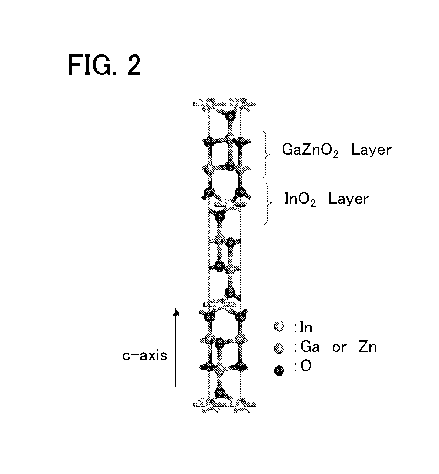
[0033]An oxide semiconductor film according to this embodiment which contains indium (In), gallium (Ga), and zinc (Zn) includes a c-axis-aligned crystalline region aligned in the direction parallel to a normal vector of a surface where the oxide semiconductor film is formed. The composition of the c-axis-aligned crystalline region is represented by In1+δGa1−δO3(ZnO)m (0xGayO3(ZnO)m (0

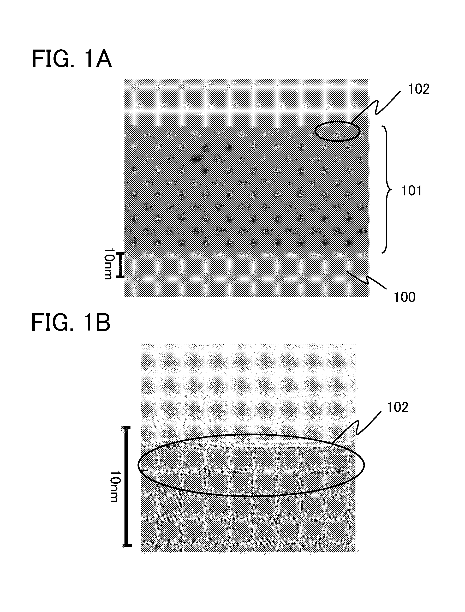
[0034]An oxide semiconductor film was actually formed, and a cross section thereof was observed with a TEM (transmission electron microscope). FIGS. 1A and 1B (cross-sectional TEM images) show the results.

[0035]A sample shown in the cross-sectional TEM image of FIG. 1A was obtained as follows. An oxide semiconductor film 101 was deposited over a substrate 100 t...

embodiment 2

[0070]In this embodiment, a method for forming the oxide semiconductor film which contains indium, gallium, and zinc and includes the c-axis-aligned crystalline region, described in Embodiment 1, and a method for manufacturing a transistor including the oxide semiconductor film will be described with reference to FIGS. 4A to 4E and FIG. 5. FIGS. 4A to 4E are cross-sectional views illustrating a manufacturing process of a top-gate transistor 320. FIG. 5 illustrates an example of a structure of a manufacturing apparatus. Unlike in Embodiment 1, a method for forming the oxide semiconductor film which includes the c-axis-aligned crystalline region through two separate steps will be described in this embodiment.

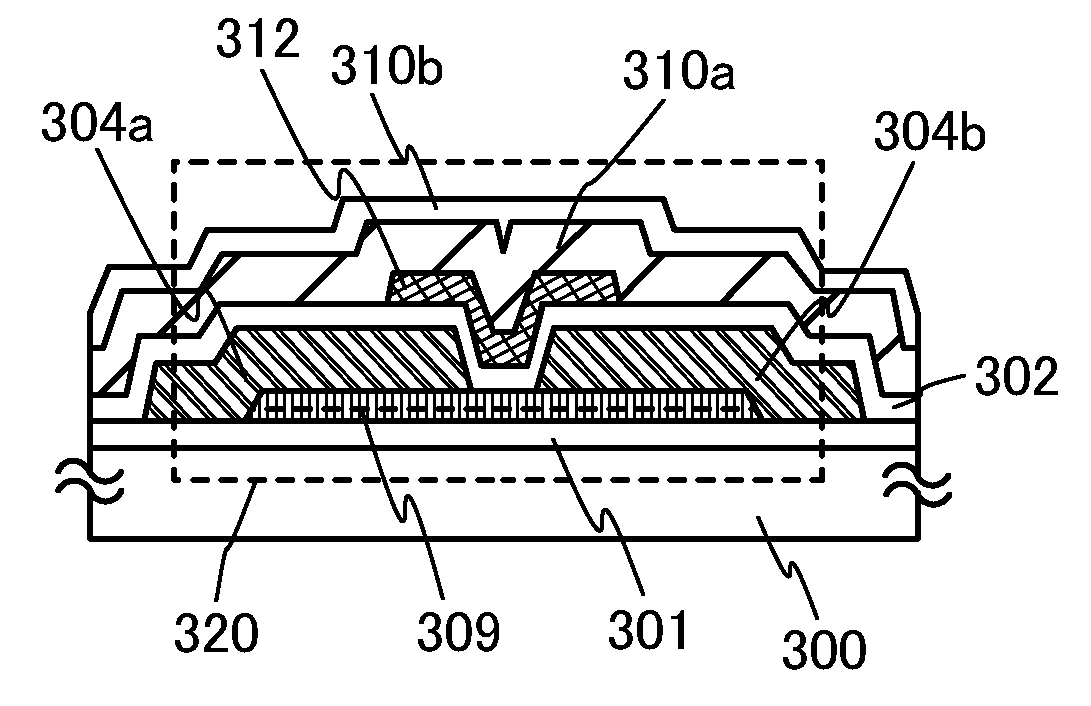
[0071]FIG. 4E is a cross-sectional view of the top-gate transistor 320. The transistor 320 includes, over a substrate 300 having an insulating surface, an insulating film 301, an oxide semiconductor film 309 including a channel formation region, a source electrode 304a, a drain el...

embodiment 3

[0115]In this embodiment, transistors whose structures are different from a structure of the top-gate transistor 320 described in Embodiment 2 will be described with reference to FIGS. 6A to 6C. Components that are similar to the components of the transistor 320 described in Embodiment 2 are denoted by the same reference numerals, and description of such components is not repeated.

[0116]In the transistor illustrated in FIGS. 6A to 6C, the oxide semiconductor film which contains indium, gallium, and zinc and includes the c-axis-aligned crystalline region, described in Embodiment 1, is used for a channel formation region, whereby the transistor can have high reliability.

[0117]A transistor 330 illustrated in FIG. 6A includes the insulating film 301 provided over the substrate 300; the source electrode 304a and the drain electrode 304b provided over the insulating film 301; the oxide semiconductor film 309 provided in contact with upper surfaces and side surfaces of the source electrode...


PUM


Abstract

To provide an oxide semiconductor film having stable electric conductivity and a highly reliable semiconductor device having stable electric characteristics by using the oxide semiconductor film. The oxide semiconductor film contains indium (In), gallium (Ga), and zinc (Zn) and includes a c-axis-aligned crystalline region aligned in the direction parallel to a normal vector of a surface where the oxide semiconductor film is formed. Further, the composition of the c-axis-aligned crystalline region is represented by In1+δGa1−δO3(ZnO)m (0<δ<1 and m=1 to 3 are satisfied), and the composition of the entire oxide semiconductor film including the c-axis-aligned crystalline region is represented by InxGayO3(ZnO)m (0<x<2, 0<y<2, and m=1 to 3 are satisfied).

Description

BACKGROUND OF THE INVENTION[0001]1. Field of the Invention[0002]The present invention relates to an oxide semiconductor film and a semiconductor device including the oxide semiconductor film.[0003]Note that the semiconductor device in this specification refers to all devices that can function by utilizing semiconductor characteristics, and electro-optic devices, semiconductor circuits, and electronic appliances are all semiconductor devices.[0004]2. Description of the Related Art[0005]Transistors formed over a glass substrate or the like are manufactured using amorphous silicon, polycrystalline silicon, or the like, as typically seen in liquid crystal display devices. A transistor manufactured using amorphous silicon can easily be formed over a larger glass substrate. However, a transistor manufactured using amorphous silicon has a disadvantage of low field-effect mobility. Although a transistor manufactured using polycrystalline silicon has high field-effect mobility, it has a disa...

Claims


Application Information

Patent Timeline
IPC IPC(8): H01L29/78H01L29/38
CPCH01L29/045H01L29/7869H01L29/78696H10K59/1213C01G15/006C01P2006/40G02F1/134309G02F1/136213G02F1/1368G02F2201/123H01L21/02565H01L21/02609H01L27/1225H01L27/1285H01L29/24H01L29/66969
Inventor TAKAHASHI, MASAHIROAKIMOTO, KENGOYAMAZAKI, SHUNPEI
Owner SEMICON ENERGY LAB CO LTD
Why Eureka
Try Eureka