Semiconductor memory device

a memory device and semiconductor technology, applied in the direction of capacitors, solid-state devices, transistors, etc., can solve the problems of large power consumption, deterioration of transistors, and significant problems, so as to improve the retention characteristic of charge accumulated in the capacitor in the dram, reduce the frequency of refresh operations, and achieve high reliability. the effect of dram

Inactive Publication Date: 2012-10-18
SEMICON ENERGY LAB CO LTD
View PDF12 Cites 17 Cited by
  • Summary
  • Abstract
  • Description
  • Claims
  • Application Information

AI Technical Summary

Benefits of technology

[0025]As described above, with the transistor with small off-state current, retention characteristic of charge accumulated in the capacitor in the DRAM can be improved. As a result, the frequency of refresh operations can be reduced.
[0026]Note that the netlike conductive film functions not only as the other of the capacitor electrodes but also as a guard ring. The function of the netlike conductive film as a guard ring can prevents electrostatic breakdown of every memory cell, so that a highly reliable DRAM with a high yield can be obtained.
[0027]In addition, according to one embodiment of the present invention, the capacitor can be formed along the side surface of the other of the pair of electrodes. The area of the side surface of the other of the pair of electrodes can be larger than the area of the top surface of the other of the pair of electrodes by controlling the thickness of the pair of electrodes. Accordingly, the area of the capacitor for obtaining a necessary capacitance can be reduced.
[0028]When the transistor with small off-state current is applied and the capacitance of the capacitor is increased, the frequency of refresh operations for retaining data in the DRAM is reduced. As a result, a semiconductor memory device with low power consumption is provided.
[0029]In addition, the capacitor of the DRAM is provided along the side surface of the other of the pair of electrodes of the transistor, whereby the capacitance of the capacitor can be increased and the area occupied by the capacitor can be reduced. As a result, a highly integrated semiconductor memory device can be provided.
[0030]In addition, the netlike conductive film which also serves as the capacitor electrode of the capacitor in the DRAM functions as a guard ring, whereby the electrostatic breakdown of every memory cell can be prevented. As a result, a highly reliable semiconductor memory device with a high yield can be provided.

Problems solved by technology

To retain data, a conventional DRAM needs to perform refresh operations at an interval of several tens of milliseconds, which results in large power consumption.
In addition, a transistor therein is frequently turned on and off; thus, deterioration of the transistor is also a problem.
This problem becomes significant as the transistor is further miniaturized and the storage capacity is further increased.

Method used


Image

  • Semiconductor memory device
  • Semiconductor memory device
  • Semiconductor memory device

Examples


embodiment 1

[0060]In this embodiment, a semiconductor memory device to which one embodiment of the present invention is applied will be described.

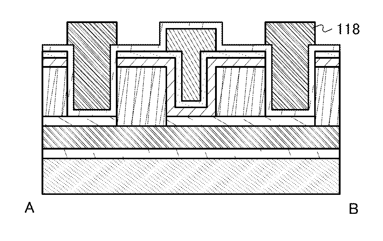
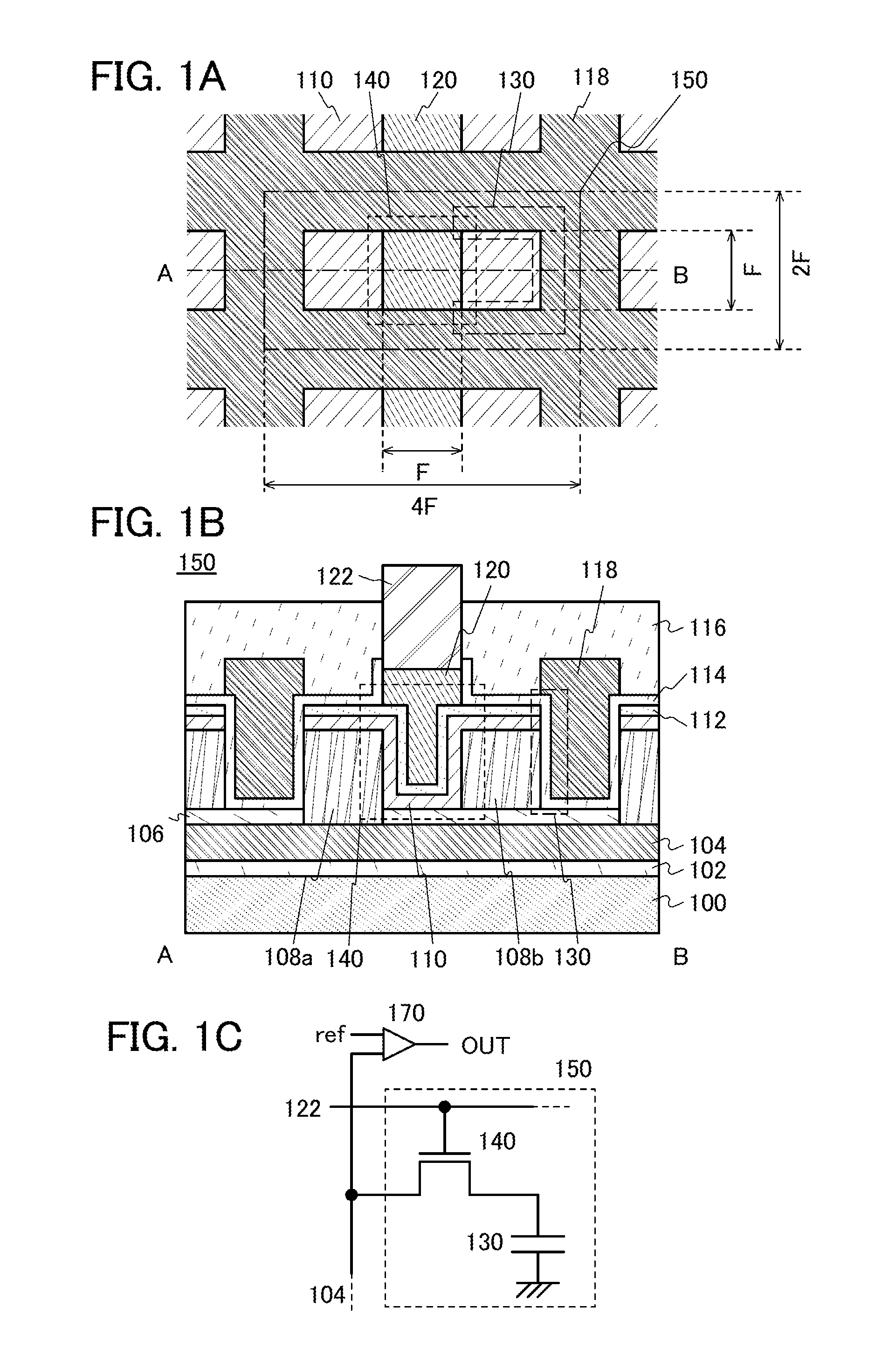
[0061]FIG. 1A is a top view illustrating part of a memory cell array that is a semiconductor memory device. FIG. 1B illustrates a cross section A-B along a dashed-dotted line A-B in FIG. 1A. In addition, FIG. 1C is a circuit diagram of a memory cell.

[0062]In FIG. 1A, a memory cell 150 includes a netlike conductive film 118, a transistor 140 including an oxide semiconductor, and a capacitor 130. Here, given that the minimum feature size is F, the size of the memory cell 150 is 2F×4F and the area thereof is 8F2.

[0063]The memory cell 150 is provided in a mesh of the netlike conductive film 118 when seen from the above. Therefore, the netlike conductive film 118 functions as a guard ring which prevents electrostatic breakdown of every memory cell.

[0064]In addition, the netlike conductive film 118 functions as a capacitor electrode of the capacitor 130. No...

embodiment 2

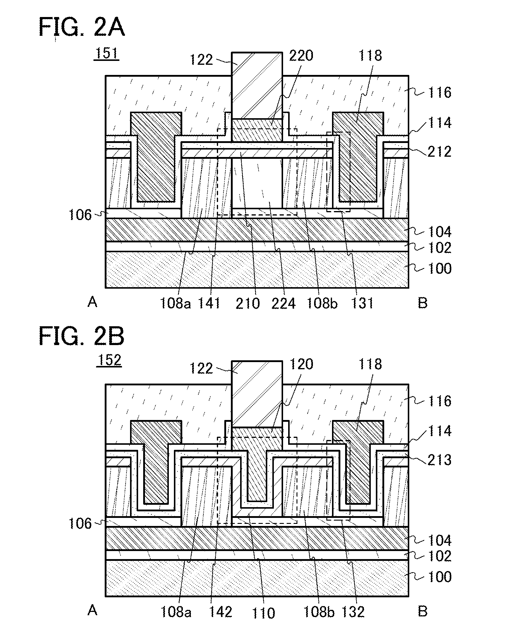
[0152]In this embodiment, memory cells having different structures from the memory cell 150 described in Embodiment 1 will be described with reference to FIGS. 2A and 2B.

[0153]A memory cell 151 illustrated in FIG. 2A is different from the memory cell 150 in that a sixth insulating film 224 which fills a space between the source electrode 108a and the drain electrode 108b is included.

[0154]Note that a capacitor 131 has the same structure as the capacitor 130.

[0155]When the sixth insulating film 224 is provided, a transistor 141 has a different shape from the transistor 140. Specifically, an oxide semiconductor film 210, a third insulating film 212, and a gate electrode 220 are provided without the oxide semiconductor film 110, the third insulating film 112, and the gate electrode 120. Here, the sixth insulating film 224 allows the structure in which the oxide semiconductor film 210, and the third insulating film 212, and the gate electrode 220 are not formed on steps formed by the so...

embodiment 3

[0165]In this embodiment, a memory cell array in which a plurality of memory cells described in Embodiment 1 or Embodiment 2 is provided will be described.

[0166]FIG. 8 illustrates a memory cell array in which memory cells according to one embodiment of the present invention are arranged in n rows and m columns.

[0167]The memory cell array includes m×n memory cells CL, m bit lines BL, and n word lines WL. The m bit lines BL are connected to respective m sense amplifiers SAmp.

[0168]The memory cell CL includes a transistor Tr and a capacitor C. The memory cell 150, the memory cell 151, or the memory cell 152 can be applied to the memory cell CL. That is, the transistor 140, the transistor 141, or the transistor 142 can be applied to the transistor Tr, and the capacitor 130, the capacitor 131, or the capacitor 132 can be applied to the capacitor C.

[0169]Next, a method for writing data and a method for reading data in the memory cell array arranged in n rows and m columns are described.

[0...


PUM


Abstract

A semiconductor memory device including a bit line, a word line, a transistor, and a capacitor is provided. The transistor includes source and drain electrodes; an oxide semiconductor film in contact with at least both top surfaces of the source and drain electrodes; a gate insulating film in contact with at least a top surface of the oxide semiconductor film; a gate electrode which overlaps with the oxide semiconductor film with the gate insulating film provided therebetween; and an insulating film covering the source and drain electrodes, the gate insulating film, and the gate electrode. The transistor is provided in a mesh of a netlike conductive film when seen from the above. Here, the drain electrode and the netlike conductive film serve as one and the other of a pair of capacitor electrodes of the capacitor. A dielectric film of the capacitor includes at least the insulating film.

Description

BACKGROUND OF THE INVENTION[0001]1. Field of the Invention[0002]The present invention relates to a semiconductor memory device which includes a circuit including a semiconductor element such as a transistor.[0003]2. Description of the Related Art[0004]A dynamic random access memory (DRAM) is a semiconductor memory device in which one bit of data can be stored with the use of one transistor and one capacitor. The DRAM has advantages such as a small area per unit memory cell, easiness in integration for modularization, and low manufacturing cost.[0005]A circuit pattern of the DRAM has been miniaturized in accordance with a scaling law in a manner similar to those of other semiconductor integrated circuits. However, when an area occupied by a transistor is reduced, most part of the area of the DRAM is occupied by a capacitor, and it is difficult to reduce the area of the capacitor. This is because the miniaturization increases leakage between a source and a drain of the transistor and ...

Claims


Application Information

Patent Timeline
Patent Type & Authority Applications(United States)
IPC IPC(8): H01L29/786
CPCH01L21/84H01L27/10876H01L27/10891H01L27/1203H01L27/0288H01L28/86H01L28/90H01L29/7869H01L28/60H10B12/053H10B12/488
Inventor SAITO, TOSHIHIKO
Owner SEMICON ENERGY LAB CO LTD
Why Eureka
Try Eureka