
Footing Reduction Using Etch-Selective Layer

a selective layer and footing technology, applied in the direction of decorative surface effects, electrical appliances, decorative arts, etc., can solve the problems of difficult control of the transfer footing shape, unexpected critical dimension (cd) changes or the like, and the difficulty of forming patterns with pitches, etc., to reduce the widened footing of the photoresist and the effect of reducing the etch ra

Active Publication Date: 2012-10-18
ASM JAPAN
View PDF1 Cites 214 Cited by
  • Summary
  • Abstract
  • Description
  • Claims
  • Application Information

AI Technical Summary

Benefits of technology

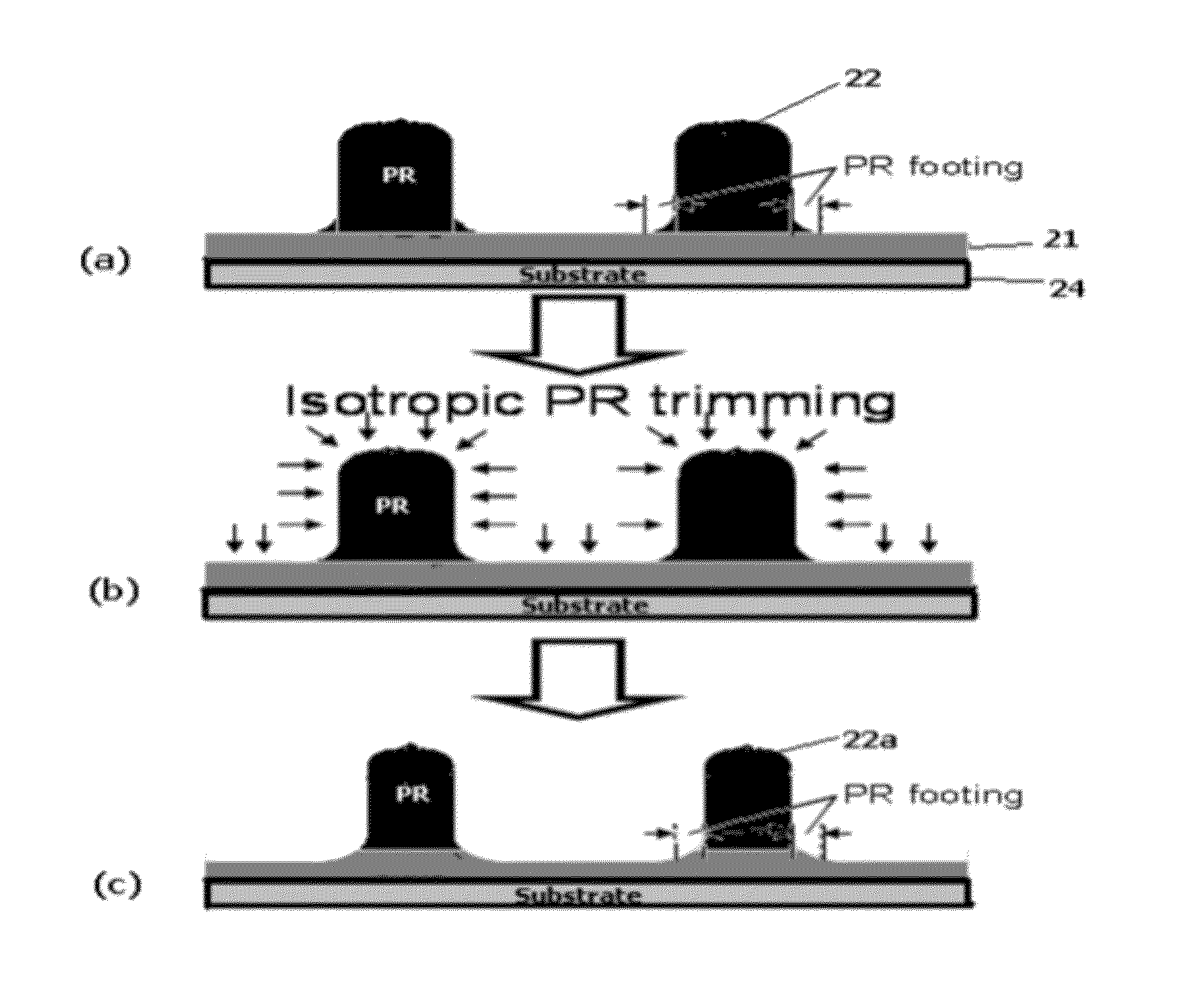
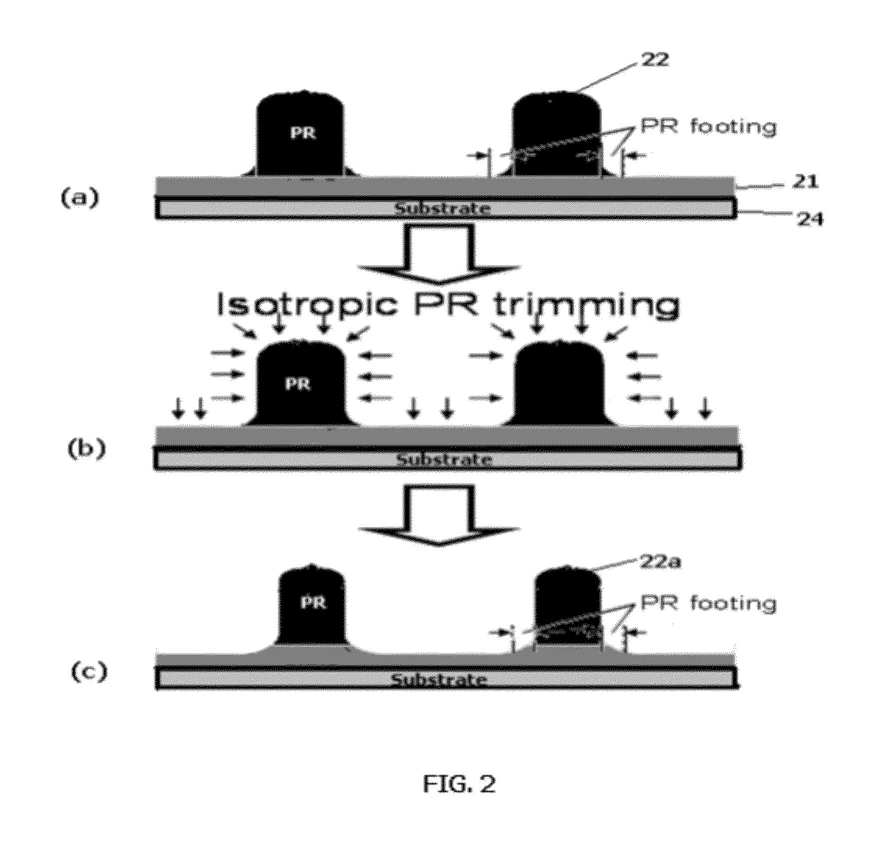
[0009]In some embodiments of the present invention, by conducting plasma irradiation prior to formation of a spacer layer to anisotropically etch a template constituted by a photoresist formed on and in contact with an etch-selective layer laminated on a substrate, said etch-selective layer has a substantially lower etch rate than that of the photoresist, thereby reducing a widened footing of the photoresist.

Problems solved by technology

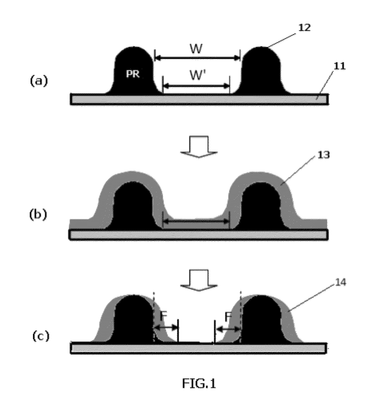
Photolithography technology has recently faced difficulty of forming patterns having pitches smaller than the submicron level.
As a result, the thickness of the side spacer at the bottom appears to be widened (F), which is significantly greater than the thickness of the side spacer itself, thereby causing unexpected critical dimension (CD) changes or the like.
However, it is still difficult to control the transferred footing shape.

Method used


Image

  • Footing Reduction Using Etch-Selective Layer
  • Footing Reduction Using Etch-Selective Layer
  • Footing Reduction Using Etch-Selective Layer

Examples


Embodiment Construction

[0020]In this disclosure, “gas” may include vaporized solids and / or liquids and may be constituted by a mixture of gases. In this disclosure, the reactant gas, the additive / carrier gas, and the precursor may be different from each other or mutually exclusive in terms of gas types, i.e., there is no overlap of gases among these categories. In some embodiments, “film” refers to a layer continuously extending in a direction perpendicular to a thickness direction substantially without pinholes to cover an entire target or concerned surface, or simply a layer covering a target or concerned surface. In some embodiments, “layer” refers to a structure having a certain thickness formed on a surface or a synonym of film. In this disclosure, any defined meanings do not necessarily exclude ordinary and customary meanings in some embodiments. In the disclosure, “substantially lower”, “substantially higher”, “substantially different”, etc. refer to a difference of at least 10%, 50%, 100%, 200%, 3...


PUM

PropertyMeasurementUnit
heat resistanceaaaaaaaaaa
widthaaaaaaaaaa

Abstract

A method of forming side spacers upwardly extending from a substrate, includes: providing a template constituted by a photoresist formed on and in contact with an etch-selective layer laminated on a substrate; anisotropically etching the template in a thickness direction with an oxygen-containing plasma to remove a footing of the photoresist and an exposed portion of the underlying layer; depositing a spacer film on the template by atomic layer deposition (ALD); and forming side spacers using the spacer film by etching. The etch-selective layer has a substantially lower etch rate than that of the photoresist.

Description

BACKGROUND[0001]1. Field of the Invention[0002]The present invention relates to semiconductor integrated circuit manufacturing and, more particularly to a method of forming side spacers, particularly on space-defined double patterning (SDDP).[0003]2. Description of the Related Art[0004]Photolithography technology has recently faced difficulty of forming patterns having pitches smaller than the submicron level. Various approaches have been studied, and one of the promising methods is space-defined double patterning (SDDP) which makes it possible to create narrow pitches beyond limitations of conventional lithography such as light source wavelength and high index immersion fluid. Generally, SDDP needs one conformal spacer film and hardmask template wherein the conformal spacer film is deposited on the template normally having convex patterns. A silicon oxide layer is commonly used as a conformal spacer, and a hardmask template is typically constituted by photoresist (PR) prepared by a...

Claims


Application Information

Patent Timeline
Patent Type & Authority Applications(United States)
IPC IPC(8): H01L21/311
CPCH01L21/0273H01L21/0276H01L21/31138H01L21/31116H01L21/0337
Inventor NAKANO, RYU
Owner ASM JAPAN
Learn More