Method for manufacturing interconnection structure and of metal nitride layer thereof

a technology of interconnection structure and metal nitride, which is applied in the direction of vacuum evaporation coating, coating, semiconductor devices, etc., can solve the problems of line distortion and film collapse, and achieve the effect of preventing the interconnection structure from film collapse and reducing the stress of the metal nitride layer or the other film of the interconnection structur

Inactive Publication Date: 2012-10-25
UNITED MICROELECTRONICS CORP
View PDF6 Cites 10 Cited by
  • Summary
  • Abstract
  • Description
  • Claims
  • Application Information

AI Technical Summary

Benefits of technology

[0025]In the present invention, the metal nitride layer is formed by the physical vapor deposition process performed at a temperature between 210° C. and 390° C., and/or on a pressure between 21 mTorr and 91 mTorr. Therefore, the film stress of the me

Problems solved by technology

Further, the films may collapse resulted

Method used


Image

  • Method for manufacturing interconnection structure and of metal nitride layer thereof
  • Method for manufacturing interconnection structure and of metal nitride layer thereof
  • Method for manufacturing interconnection structure and of metal nitride layer thereof

Examples


Embodiment Construction

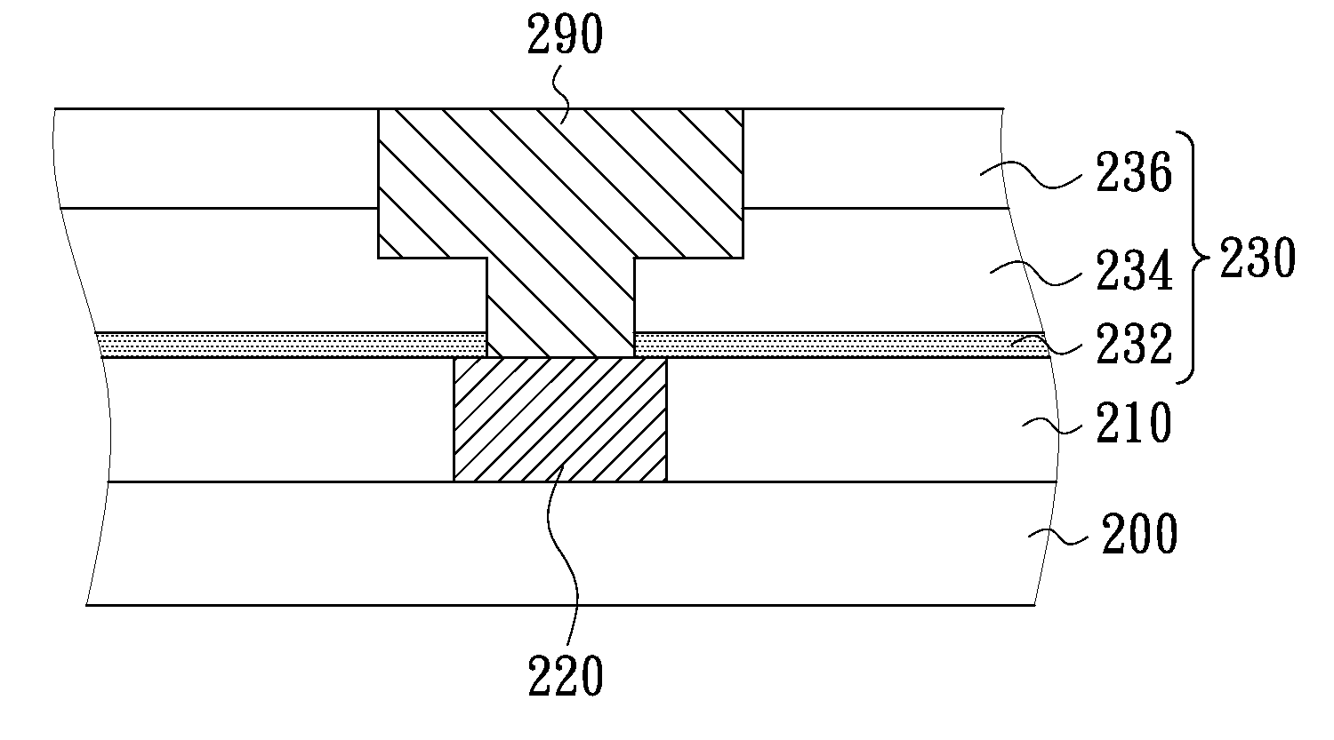
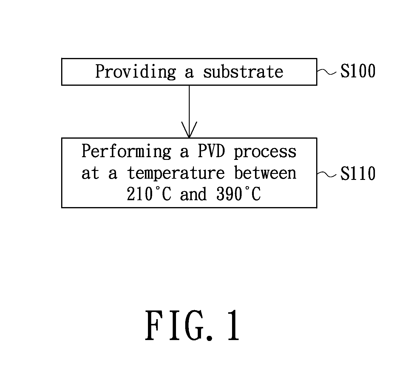
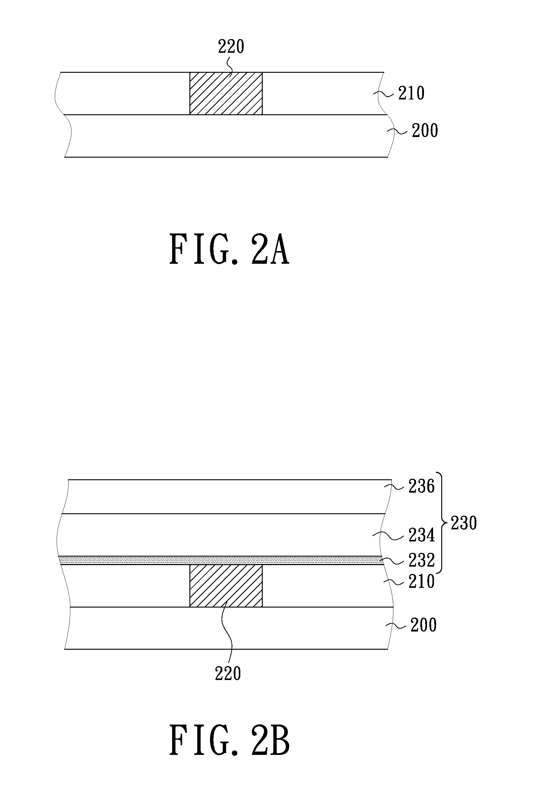
[0029]FIG. 1 is a flow chart of a method for manufacturing a metal nitride layer according to an embodiment of the present invention. Referring to FIG. 1, in the step S100, a substrate is provided. Next, in the step S110, a physical vapor deposition process is performed at a temperature between 210° C. and 390° C. to form a metal nitride layer on the substrate. In this embodiment, the physical vapor deposition process is, for example, a reactive sputtering process. Specifically, a target which used in the reactive sputtering process is made of titanium and the gases which used in the process include inert gas (e.g., argon) and nitrogen. The titanium atom fallen from the target due to be hit by the inert gas are reactive to each other, so as to deposit a titanium nitride layer on the substrate.

[0030]In the prior art skill, the metal nitride layer is deposited through a deposition process at room temperature (about 25° C.), so as to has a film stress about 2.5 GPa. In this embodiment,...


PUM

PropertyMeasurementUnit
Temperatureaaaaaaaaaa
Pressureaaaaaaaaaa

Abstract

A method for manufacturing a metal nitride layer including the following steps is provided. Firstly, a substrate is provided. Then, a physical vapor deposition process is performed at a temperature between 210° C. and 390° C. to form a metal nitride layer on the substrate. Also, the physical vapor deposition process can be performed on a pressure between 21 mTorr and 91 mTorr. The method can be used in the manufacturing process of an interconnection structure for decreasing the film stress of the metal nitride layer. Therefore, the interconnection structure can be prevented from line distortion and film collapse.

Description

FIELD OF THE INVENTION[0001]The present invention relates to a semiconductor process, and more particularly to methods for manufacturing an interconnection structure and for manufacturing a metal nitride layer thereof.DESCRIPTION OF THE RELATED ART[0002]Since copper has a relatively low resistance value (30% less than aluminum) and a relatively good electro-migration resistance, and the low-k material, the porous low-k material and the ultra low-k material can make for reducing RC delay between metal wires, copper dual damascene technique with abovementioned low-k material is the best solution of metal interconnection for fabricating logic integrated circuit chips with high integration.[0003]Generally, a metal hard mask (so-called MHM) is formed on the low-k dielectric layer to protect it from damage due to a chemical mechanical polishing (so-called CMP) process in the process of manufacturing the dual damascene interconnection structure. The metal hard mask is usually made by titan...

Claims


Application Information

Patent Timeline
IPC IPC(8): H01L21/768H01L21/28
CPCH01L21/2855C23C14/0641H01L21/7681H01L21/31144
Inventor LIN, CHUN-LINGLIN, CHIN-FUHSU, CHI-MAO
Owner UNITED MICROELECTRONICS CORP
Why Eureka
Try Eureka