Unlock instant, AI-driven research and patent intelligence for your innovation.

Lateral-epitaxial-overgrowth thin-film LED with nanoscale-roughened structure and method for fabricating the same

Inactive Publication Date: 2012-11-01
NAT CHIAO TUNG UNIV
View PDF2 Cites 5 Cited by
  • Summary
  • Abstract
  • Description
  • Claims
  • Application Information

AI Technical Summary

Benefits of technology

[0006]The primary objective of the present invention is to provide a lateral-epitaxial-overgrowth thin-film LED with a nanoscale-roughened structure and a method for fabricating the same, wherein the semiconductor structure thereof is grown in a lateral-epitaxial-overgrowth way on an epitaxy substrate having a nanoscale-patterned silicon oxide layer, whereby are inhibited the stacking faults in epitaxially growing the semiconductor structure, decreased the thread dislocation density, and increased the crystallization quality of the light-emitting semiconductor layer.
[0007]Another objective of the present invention is to provide a lateral-epitaxial-overgrowth thin-film LED with a nanoscale-roughened structure and a method for fabricating the same, which can promote the external quantum efficiency without roughening the light-outgoing face of the semiconductor structure once again.
[0008]A further objective of the present invention is to provide a lateral-epitaxial-overgrowth thin-film LED with a nanoscale-roughened structure and a method for fabricating the same, which needn't use photolithography to etch patterns, whereby is greatly reduced the complexity and cost of fabrication.

Problems solved by technology

Using a laser lift-off method to fabricate GaN LED (Light Emitting Diode) can effectively improve heat radiation in chip level and obviously reduce the efficiency droop caused by poor heat radiation.
Further, the laser lift-off method also increases the light-emitting area of LED.
In a paper “Effects of Laser Sources on the Reverse-Bias Leakages of Laser Lift-Off Gan-Based Light-Emitting Diodes”, by Yewchung Sermon Wu, Ji-Hao Cheng, and Wei Chih Peng, in APPLIED PHYSICS LETTERS 90, 251110 (2007), it was found that the stress release caused by the laser lift-off method increases dislocations, which not only decreases the light-emitting efficiency but also shortens the service life.
Although the prior art instructed the methods for promoting the epitaxy quality of GaN and increasing the light extraction efficiency thereof, the process is too complicated to realize.
However, the conventional technology uses photolithography to etch patterns, which increases the fabrication complexity and thus raises the fabrication cost.

Method used


Image

  • Lateral-epitaxial-overgrowth thin-film LED with nanoscale-roughened structure and method for fabricating the same
  • Lateral-epitaxial-overgrowth thin-film LED with nanoscale-roughened structure and method for fabricating the same
  • Lateral-epitaxial-overgrowth thin-film LED with nanoscale-roughened structure and method for fabricating the same

Examples


Embodiment Construction

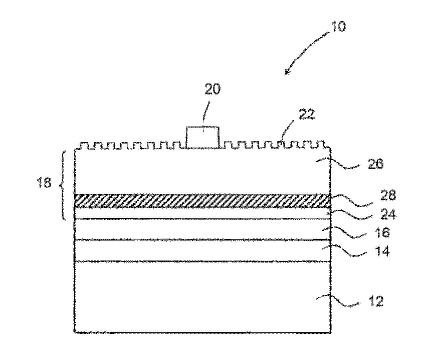
[0020]Refer to FIG. 1 for the structure of a lateral-epitaxial-overgrowth thin-film LED with a nanoscale-roughened structure according to one embodiment of the present invention. The lateral-epitaxial-overgrowth thin-film LED 10 with a nanoscale-roughened structure of the present invention comprises a substrate 12; a metal bonding layer 14 formed on the substrate 12; a first electrode 16 formed on the metal bonding layer 14; a semiconductor structure 18 formed on the first electrode 16; and a second electrode 20 formed on the semiconductor structure 18, wherein the upper surface of the semiconductor structure 18 has a nanoscale-roughened structure 22 except the area covered by the second electrode 20.

[0021]The metal bonding layer 14 is a dual-layer structure having a titanium layer and a gold layer bottom up. The first electrode 16 is a three-layer structure having a gold layer, a platinum layer and a chromium layer bottom up. Thus, the gold layer of the metal bonding layer 14 conta...


PUM


Abstract

The present invention discloses a lateral-epitaxial-overgrowth thin-film LED with a nanoscale-roughened structure and a method for fabricating the same. The lateral-epitaxial-overgrowth thin-film LED with a nanoscale-roughened structure comprises a substrate, a metal bonding layer formed on the substrate, a first electrode formed on the metal bonding layer, a semiconductor structure formed on the first electrode with a lateral-epitaxial-growth technology, and a second electrode formed on the semiconductor structure, wherein a nanoscale-roughened structure is formed on the semiconductor structure except the region covered by the second electrode. The present invention uses lateral epitaxial growth to effectively inhibit the stacking faults and reduce the thread dislocation density in the semiconductor structure to improve the crystallization quality of the light-emitting layer and reduce leakage current. Meanwhile, the surface roughened structure on the semiconductor structure can promote the external quantum efficiency.

Description

BACKGROUND OF THE INVENTION[0001]1. Field of the Invention[0002]The present invention relates to a thin-film LED and a method for fabricating the same, particularly to a lateral-epitaxial-overgrowth thin-film LED with a nanoscale-roughened structure and a method for fabricating the same.[0003]2. Description of the Related Art[0004]Using a laser lift-off method to fabricate GaN LED (Light Emitting Diode) can effectively improve heat radiation in chip level and obviously reduce the efficiency droop caused by poor heat radiation. Further, the laser lift-off method also increases the light-emitting area of LED. Therefore, the laser lift-off method has been the mainstream technology to fabricate high-power LED. In a paper “Effects of Laser Sources on the Reverse-Bias Leakages of Laser Lift-Off Gan-Based Light-Emitting Diodes”, by Yewchung Sermon Wu, Ji-Hao Cheng, and Wei Chih Peng, in APPLIED PHYSICS LETTERS 90, 251110 (2007), it was found that the stress release caused by the laser lift...

Claims


Application Information

Patent Timeline
IPC IPC(8): H01L33/04
CPCH01L33/007H01L33/0079H01L33/06H01L33/32H01L33/0095H01L33/22H01L33/0093
Inventor LEE, CHIA-YUWANG, CHAO-HSUNCHIU, CHING-HSUEHKUO, HAO-CHUNG
Owner NAT CHIAO TUNG UNIV