Gate stack structure with etch stop layer and manufacturing process thereof

a technology of etch stop layer and stack structure, which is applied in the direction of basic electric elements, electrical apparatus, semiconductor devices, etc., can solve the problems of loss of the barrier layer underneath the etch stop layer, adverse effects on performance, yield and reliability of the final product, etc., and achieve the effect of increasing formation speed and thickness

Active Publication Date: 2012-11-01
UNITED MICROELECTRONICS CORP
View PDF4 Cites 21 Cited by
  • Summary
  • Abstract
  • Description
  • Claims
  • Application Information

AI Technical Summary

Benefits of technology

[0003]Therefore, the object of the present invention is to provide a gate stack structure with an etch stop layer. For repairing a damaged surface of a barrier layer, a repair layer whose material and electrical property are similar to the barrier layer is formed on the barrier layer. By means of the repair layer, an etch stop layer is formed within a trench of the gate stack structure at increased formation speed and thickness in a subsequent process. As a consequence, a current leakage problem is eliminated.

Problems solved by technology

However, since the efficacy of using such etch stop layer to prevent from over-etching the work function metal layer is usually unsatisfied, a barrier layer underneath the etch stop layer may be lost.
Under this circumstance, the performance, yield and reliability of the final product will be adversely affected.

Method used


Image

  • Gate stack structure with etch stop layer and manufacturing process thereof
  • Gate stack structure with etch stop layer and manufacturing process thereof
  • Gate stack structure with etch stop layer and manufacturing process thereof

Examples


Embodiment Construction

[0012]The present invention will now be described more specifically with reference to the following embodiments. It is to be noted that the following descriptions of preferred embodiments of this invention are presented herein for purpose of illustration and description only. It is not intended to be exhaustive or to be limited to the precise form disclosed.

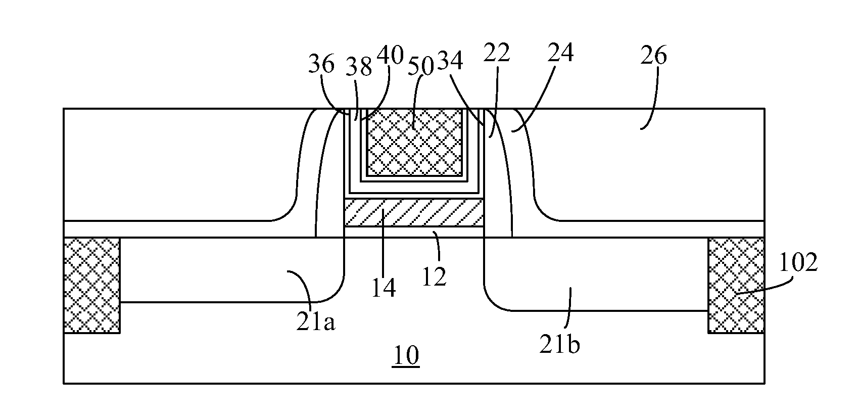
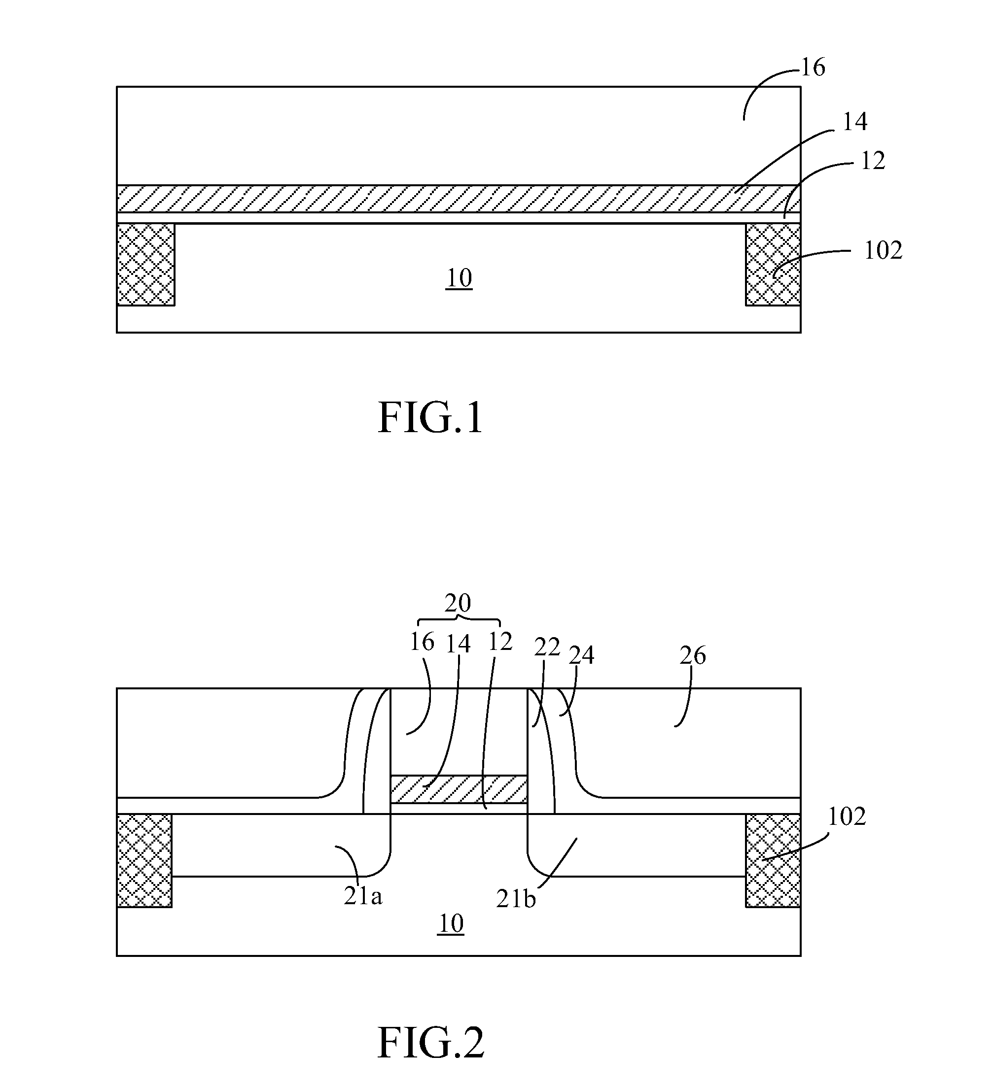
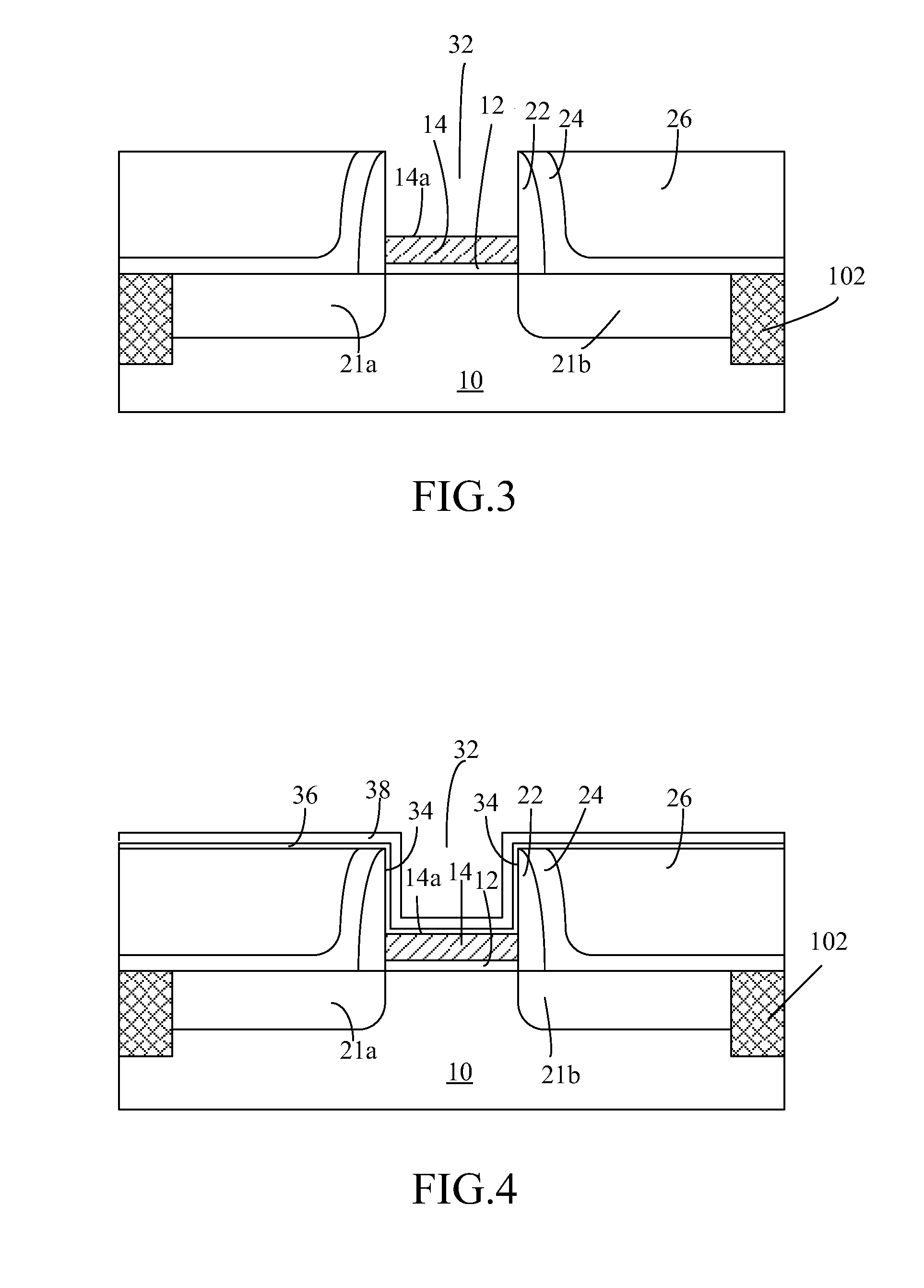
[0013]FIG. 1 schematically illustrates a gate dielectric layer, a barrier layer and a dummy polysilicon layer formed on a substrate. FIG. 2 schematically illustrates a gate stack structure formed over the substrate and a contact etch stop layer and an interlayer dielectric layer formed over the gate stack structure. FIG. 3 schematically illustrates the gate stack structure whose dummy polysilicon layer is removed. FIG. 4 schematically illustrates a repair layer and an etch stop layer formed within the trench of the gate stack structure. FIG. 5 schematically illustrates an N-type work function metal layer and a low-resistance meta...


PUM


Abstract

A gate stack structure with an etch stop layer is provided. The gate stack structure is formed over a substrate. A spacer is formed on a sidewall of the gate stack structure. The gate stack structure includes a gate dielectric layer, a barrier layer, a repair layer and the etch stop layer. The gate dielectric layer is formed on the substrate. The barrier layer is formed on the gate dielectric layer. The barrier layer and an inner sidewall of the spacer collectively define a trench. The repair layer is formed on the barrier layer and an inner wall of the trench. The etch stop layer is formed on the repair layer.

Description

FIELD OF THE INVENTION[0001]The present invention relates to a gate stack structure with an etch stop layer, and more particularly to a gate stack structure with an etch stop layer at high formation speed and high coverage percentage. The present invention also relates to a manufacturing process of the etch stop layer.BACKGROUND OF THE INVENTION[0002]During the process of fabricating a gate stack structure of a complementary metal-oxide-semiconductor (CMOS), tantalum nitride (TaN) is usually used as an etch stop layer to prevent from over-etching a work function metal layer. However, since the efficacy of using such etch stop layer to prevent from over-etching the work function metal layer is usually unsatisfied, a barrier layer underneath the etch stop layer may be lost. Under this circumstance, the performance, yield and reliability of the final product will be adversely affected.SUMMARY OF THE INVENTION[0003]Therefore, the object of the present invention is to provide a gate stac...

Claims


Application Information

Patent Timeline
Patent Type & Authority Applications(United States)
IPC IPC(8): H01L29/772H01L21/28
CPCH01L29/4966H01L29/66545H01L29/401H01L21/28008H01L29/78H01L21/31144
Inventor LIN, KUN-HSIENHUANG, HSIN-FUHSU, CHI-MAOLIN, CHIN-FUWU, CHUN-YUAN
Owner UNITED MICROELECTRONICS CORP
Why Eureka
Try Eureka