Preparation method of N-type crystalline silicon cell, cell thereof, battery and system

A technology of crystalline silicon cells and crystalline silicon, applied in the field of solar cells, can solve the problems of incomplete removal, influence of PN junction quality, difficulty in guaranteeing phosphorus diffusion, etc., achieve high open circuit voltage and photoelectric conversion efficiency, good quality, and process Simple and Controllable Effects

Inactive Publication Date: 2017-05-10
TAIZHOU ZHONGLAI PHOTOELECTRIC TECH CO LTD
View PDF6 Cites 2 Cited by
  • Summary
  • Abstract
  • Description
  • Claims
  • Application Information

AI Technical Summary

Problems solved by technology

The disadvantages of this solution are: 1) spin coating and drying equipment need to be added; 2) in order to meet the requirements of spin coating, certain organic solvents or surfactants must be added to the boron source, and these substances cannot be completely removed after drying. At the same time, some pollution is inevitably introduced in the spin coating operation, which will affect the quality of the PN junction formed by subsequent high-temperature doping; 3) The front BSG layer formed by the spin coating method is relatively loose, and it is difficult to completely block the diffusion of phosphorus

Method used


Image

  • Preparation method of N-type crystalline silicon cell, cell thereof, battery and system
  • Preparation method of N-type crystalline silicon cell, cell thereof, battery and system
  • Preparation method of N-type crystalline silicon cell, cell thereof, battery and system

Examples


Embodiment Construction

[0044] The present invention will be described in detail below in conjunction with the embodiments and the accompanying drawings. It should be noted that the described embodiments are only intended to facilitate the understanding of the present invention, rather than limiting it in any way.

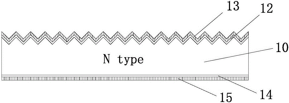
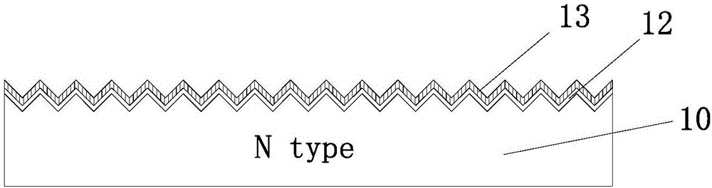
[0045] see Figure 1 to Figure 7 As shown, a method for preparing an N-type crystalline silicon battery provided in this embodiment includes the following steps:

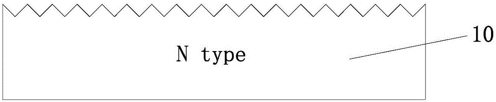
[0046] (1), select the N-type crystalline silicon substrate 10 of 156.75mm * 156.75mm, and do texture processing to the front surface of the N-type crystalline silicon substrate 10; the resistivity of the N-type crystalline silicon substrate 10 is 0.2~15Ω·cm, Preferably 0.5-5Ω·cm; the thickness of the N-type crystalline silicon substrate 10 is 50-300 μm, preferably 80-200 μm; the battery structure after this step is as follows figure 1 shown.

[0047] (2) Put the N-type crystalline silicon substrate 10 treated in step (1) int...


PUM

PropertyMeasurementUnit
thicknessaaaaaaaaaa
thicknessaaaaaaaaaa
thicknessaaaaaaaaaa

Abstract

The present invention relates to a preparation method of an N-type crystalline silicon cell, a cell thereof, a battery and a system. The preparation method of the N-type crystalline silicon cell comprises the following steps of texturing, conducting the boron diffusion operation on the front surface to form a borosilicate glass layer, conducting the etching and boron diffusion operation on the back surface, enabling edge isolation, cleaning, plating a film, printing and sintering. The invention has the following beneficial effects: through adjusting the process parameters of boron diffusion, the borosilicate glass layer formed through boron diffusion has the ability of preventing the phosphorous diffusion, so that a simple N-type crystalline silicon cell fabrication process is developed; the process is simple, controllable, low in equipment investment; based on the diffusion method, formed PN junctions are less in pollution and better in quality compared with PN junctions formed through the boron- source spin coating process or the screen printing process; the diffusion coefficient of boron in silicon dioxide is higher than that of silicon, so that a thick borosilicate glass layer facilitates the reduction of the boron concentration on the surface of a p + region so as to reduce the surface recombination and improve the open-circuit voltage. The prepared N-type crystalline silicon cell is higher in open-circuit voltage and better in photoelectric conversion efficiency.

Description

technical field [0001] The invention relates to the technical field of solar cells, in particular to a method for preparing an N-type crystalline silicon cell and the cell, component and system thereof. Background technique [0002] A solar cell is a semiconductor device that converts solar energy into electricity. At present, the mainstream products in the industry are P-type crystalline silicon solar cells. The battery process is simple, but it has a light-induced decay effect, that is, the efficiency of the battery will gradually decay with time, which is mainly due to the combination of boron atoms doped into the P-type silicon substrate and oxygen atoms in the substrate. Produces boron-oxygen pair results. Studies have shown that the boron-oxygen pair acts as a carrier trap, reducing the minority carrier lifetime, which leads to the attenuation of the photoelectric conversion efficiency of the battery. Compared with P-type crystalline silicon solar cells, N-type crys...

Claims


Application Information

Patent Timeline
Patent Type & Authority Applications(China)
IPC IPC(8): H01L31/18H01L31/068
CPCH01L31/068H01L31/1804Y02E10/547Y02P70/50
Inventor 林建伟刘志锋季根华孙玉海刘勇张育政
Owner TAIZHOU ZHONGLAI PHOTOELECTRIC TECH CO LTD
Why Eureka
Try Eureka