
Eureka
For R&D, Eureka makes reading and utilizing patents & technical documents easy.
Eureka AIR
Designed for self-driven R&D workflows. Generate viable solutions, solve complex R&D challenges, empower your innovation with AI.

Eureka Materials
Designed for material experts only. Revolutionize your material R&D, from search, analyze, to developing new materials.

TechResearch
Generate reliable direction feasibility study reports for your R&D in just a few steps.

TechSeek
Discover and master advanced knowledge NOW. Basics, ideas, possibilities, all at once.

TechMind
As an expert in R&D Theories, TechMind can generates customized viable solutions instantly.

TechRisk
Analyze your overall solution with one click, know your potential R&D risks in advance.

TechMonitor
Get weekly tech updates, stay abreast of the latest tech innovations and key insights.
Semiconductor device and method of manufacturing the same
- Summary
- Abstract
- Description
- Claims
- Application Information
AI Technical Summary
Benefits of technology
Problems solved by technology
Method used
Image

Examples
first embodiment
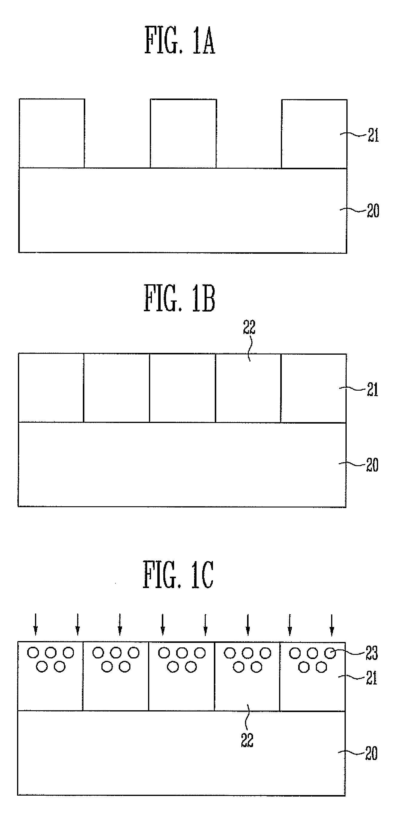
[0026]In the first embodiment, such an example that the ion implantation process is performed after the polishing process is described. However, the polishing process may be performed after the ion implantation process. If the polishing process is performed after the ion implantation process, it is preferred that the Rp point, the energy, and the doping concentration be controlled so that the inert element or the nonmetallic element 23 remains within the Cu wiring even after the polishing process. For example, it is preferred that the Rp point be adjusted to become 500 nm or higher and the energy and the doping concentration used in the ion implantation process be increased.
[0027]In the first embodiment, the inert element or the nonmetallic element 23 remains not only in the Cu wiring, but also in the interlayer dielectric layer 21. However, the inert element or the nonmetallic element 23 does not generate such a bridge because the element has non-conductivity, although they remain ...
second embodiment
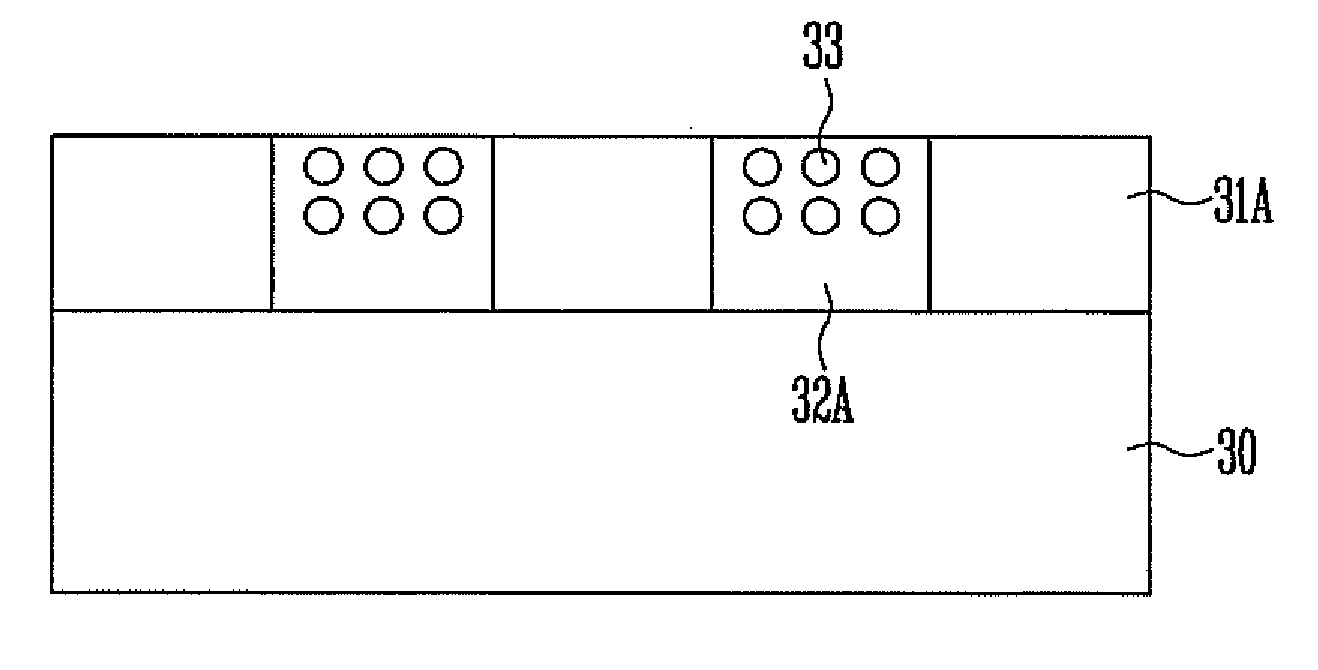
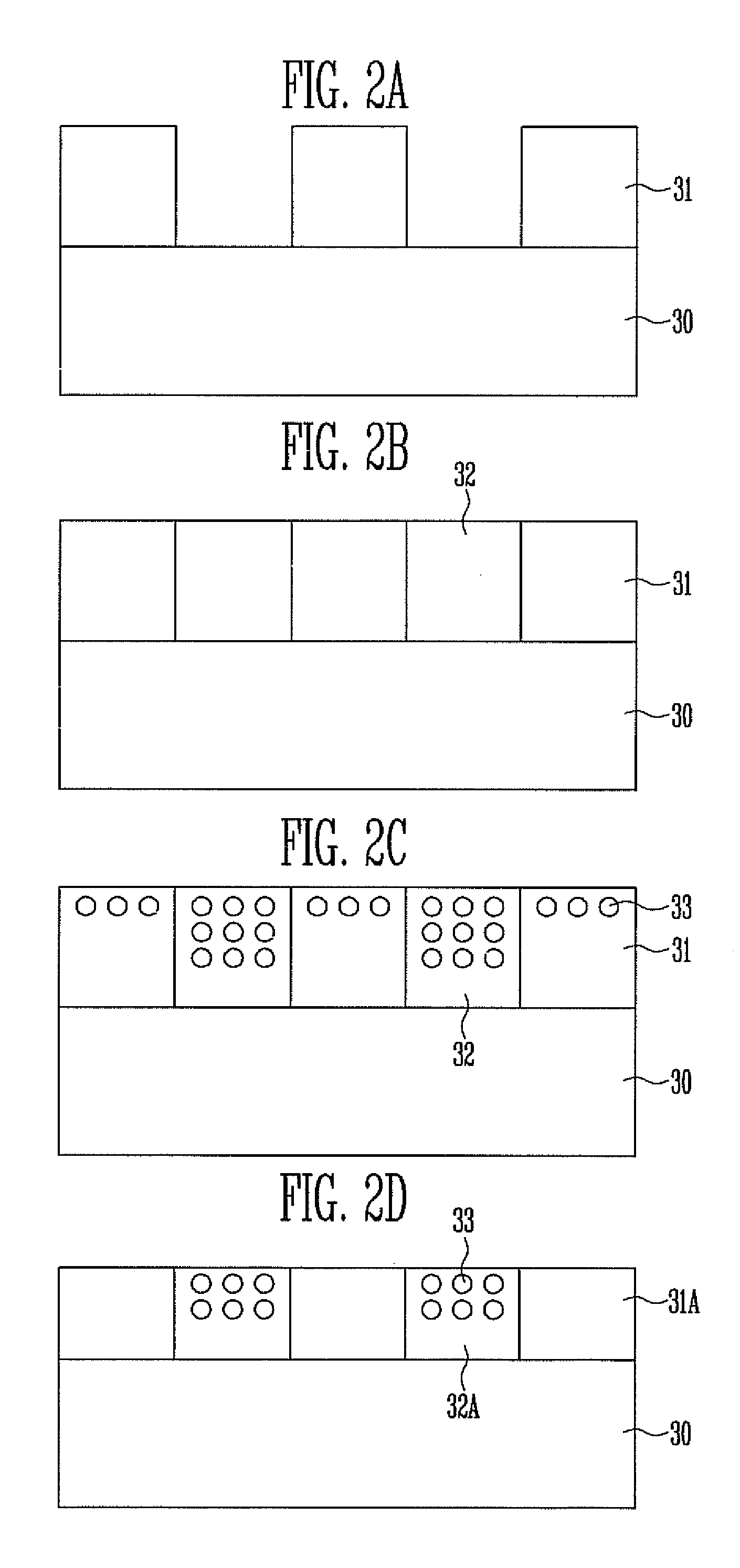
[0039]In the second embodiment, such an example that the primary polishing process, the ion implantation process, and the secondary polishing process are sequentially formed is described. In some embodiments, only the secondary polishing process may be performed without the primary polishing process. In this case, it is preferred that the Rp point be adjusted to become 500 nm or higher and the energy and doping concentration used in ion implantation process be increased so that the metallic element 33 remain in the Cu wiring even after the secondary polishing process.
[0040]Meanwhile, the Cu wiring may be formed in the manner obtained by combining the first embodiment and the second embodiment.
[0041]For example, after the inert element or the nonmetallic element is injected onto a surface of the Cu layer 22 or 32 through a primary ion implantation process, the metallic element may be secondarily injected onto a surface of the Cu layer 22 or 32 into which the inert element or the nonm...
PUM
 Abstract
Description
Claims
Application Information
 - R&D Engineer
- R&D Manager
- IP Professional
- Industry Leading Data Capabilities
- Powerful AI technology
- Patent DNA Extraction
Browse by: Latest US Patents, China's latest patents, Technical Efficacy Thesaurus, Application Domain, Technology Topic, Popular Technical Reports.
© 2024 PatSnap. All rights reserved.Legal|Privacy policy|Modern Slavery Act Transparency Statement|Sitemap|About US| Contact US: help@patsnap.com