Semiconductor chamber apparatus for dielectric processing

a dielectric processing and chamber technology, applied in electrical apparatus, basic electric elements, electric discharge tubes, etc., can solve the problems of inability to readily remove silicon, consumption of silicon oxide material, associated production of solid residues, etc., and achieve the effect of improving the throughput of a processing system and increasing the number of processing chambers

Inactive Publication Date: 2012-11-15
APPLIED MATERIALS INC
View PDF18 Cites 244 Cited by
  • Summary
  • Abstract
  • Description
  • Claims
  • Application Information

AI Technical Summary

Benefits of technology

[0007]Systems and chambers for processing dielectric films on substrates are described. Vertical combo chambers include two separate processing chambers vertically arranged in a processing stack. A top processing chamber is configured to process the substrate at relatively low substrate temperature. A robot is, configured to remove a substrate from the top processing chamber and change height before placing the substrate in a bottom processing chamber. The bottom processing chamber is configured to anneal the substrate to further process the dielectric film. The vertical stacking increases the number of processing chambers which can be included on a single processing system. The separation of the bottom (annealing or curing) chamber and the top chamber allows the top chamber to remain at a low temperature which hastens the start of a process conducted on a new wafer transferred into the top chamber. This configuration of vertical-combo chamber can be used for depositing a dielectric film in the top chamber and then curing the film in the bottom chamber. The configuration is also helpful for dielectric removal processes which create solid residue, in which case the bottom chamber is used to sublimate the solid residue. The separation limits or substantially eliminates the amount of solid residue which accumulates in the top chamber. Simultaneous processing, thermal separation and contamination control afforded by the design of the vertical combo chambers improve the throughput of a processing system.

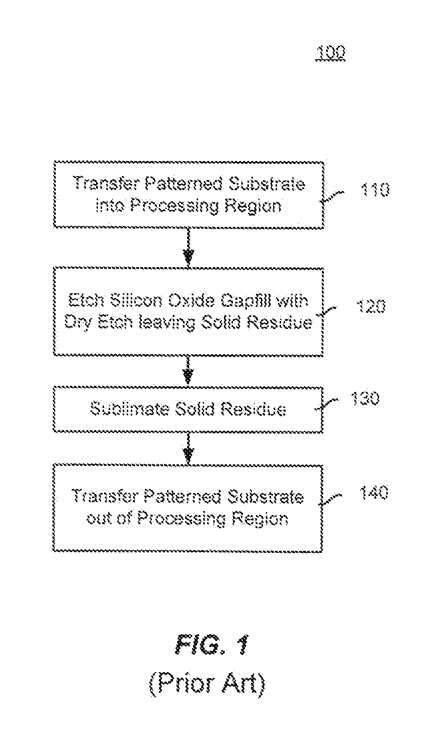
Problems solved by technology

The process is selective towards silicon oxide layers but does not readily remove silicon regardless of whether the silicon is amorphous, crystalline or polycrystalline.
The selective process results in the consumption of silicon oxide material (e.g. from within trenches) and the associated production of solid residue above any remaining silicon oxide.

Method used


Image

  • Semiconductor chamber apparatus for dielectric processing
  • Semiconductor chamber apparatus for dielectric processing
  • Semiconductor chamber apparatus for dielectric processing

Examples


Embodiment Construction

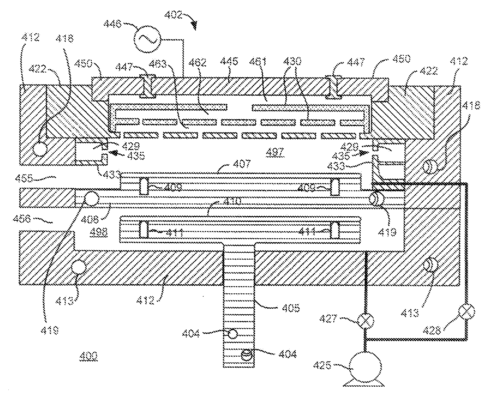
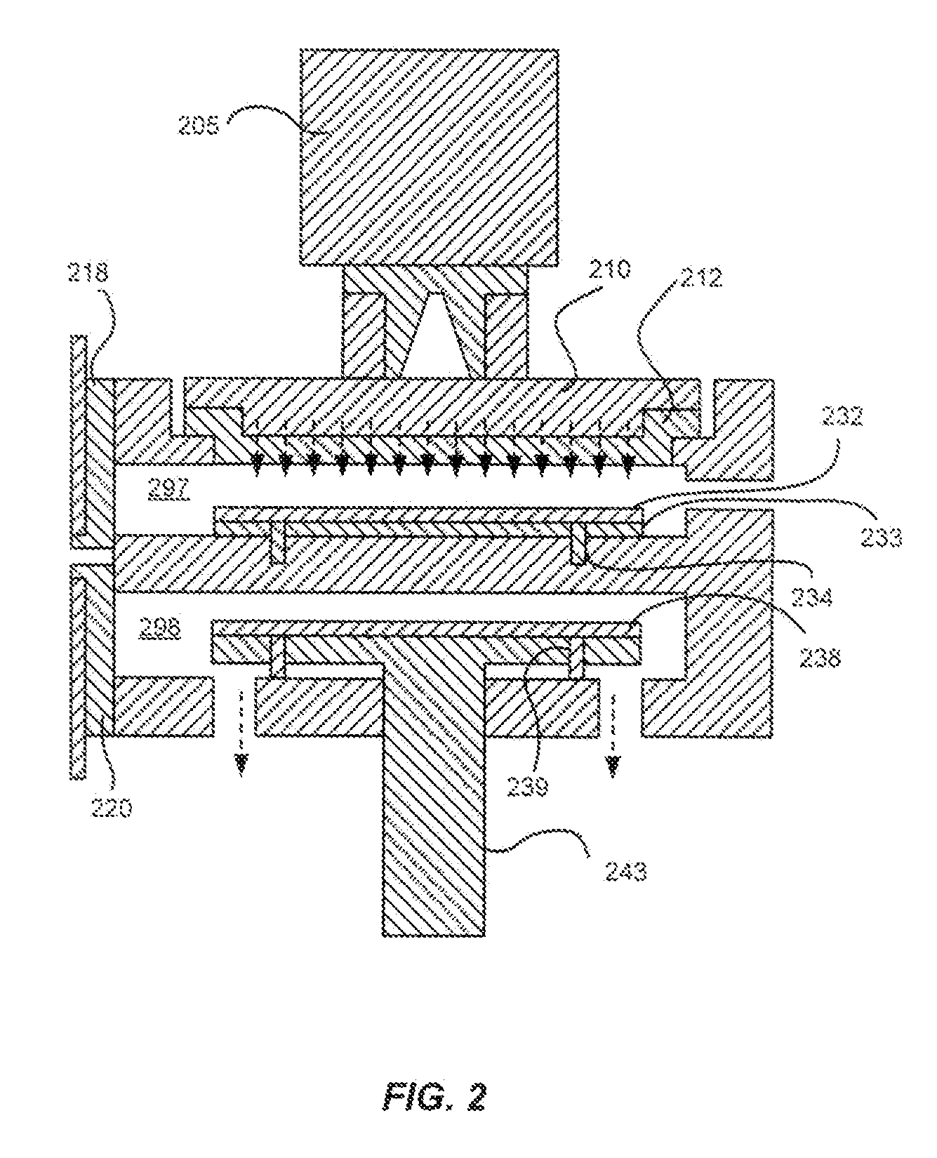
[0017]Systems and chambers for processing dielectric films on substrates are described. Vertical combo chambers include two separate processing chambers vertically arranged in a processing stack. A top processing chamber is configured to process the substrate at relatively low substrate temperature. A robot is configured to remove a substrate from the top processing chamber and change height before placing the substrate in a bottom processing chamber. The bottom processing chamber is configured to anneal the substrate to further process the dielectric film. The vertical stacking increases the number of processing chambers which can be included on a single processing system. The separation of the bottom (annealing or curing) chamber and the top chamber allows the top chamber to remain at a low temperature which hastens the start of a process conducted on a new wafer transferred into the top chamber. This configuration of vertical-combo chamber can be used for depositing a dielectric ...


PUM

PropertyMeasurementUnit
temperatureaaaaaaaaaa

Abstract

Systems and chambers for processing dielectric films on substrates are described. Vertical combo chambers include two separate processing chambers vertically arranged in a processing stack. A top processing chamber is configured to process the substrate at relatively low substrate temperature. A robot is configured to remove a substrate from the top processing chamber and change height before placing the substrate in a bottom processing chamber. The bottom processing chamber is configured to anneal the substrate to further process the dielectric film. The vertical stacking increases the number of processing chambers which can be included on a single processing system. The separation of the bottom (annealing or curing) chamber and the top chamber allows the top chamber to remain at a low temperature which hastens the start of a process conducted on a new wafer transferred into the top chamber. This configuration of vertical-combo chamber can be used for depositing a dielectric film in the top chamber and then curing the film in the bottom chamber. The configuration is also helpful for dielectric removal processes which create solid residue, in which case the bottom chamber is used to sublimate the solid residue. The separation limits or substantially eliminates the amount of solid residue which accumulates in the top chamber. Simultaneous processing, thermal separation and contamination control afforded by the design of the vertical combo chambers improve the throughput of a processing system.

Description

CROSS-REFERENCES TO RELATED APPLICATIONS[0001]This application claims the benefit of U.S. Prov. Pat. App. No. 61 / 484,284 filed May 10, 2011, and titled “STACKED CHAMBER FOR IMPROVED THROUGHPUT LOW TEMPERATURE ETCH,” which is entirely incorporated herein by reference for all purposes.BACKGROUND OF THE INVENTION[0002]Integrated circuits are made possible by processes which produce intricately patterned material layers on substrate surfaces. Producing patterned material on a substrate requires controlled methods for removal of exposed material. Chemical etching is used for a variety of purposes including transferring a pattern in'photoresist into underlying layers, thinning layers or thinning lateral dimensions of features already present on the surface. Often it is desirable to have an etch process which etches one material faster than another helping e.g. a pattern transfer process proceed. Such an etch process is said to be selective to the first material. As a result of the diversi...

Claims


Application Information

Patent Timeline
Patent Type & Authority Applications(United States)
IPC IPC(8): H01L21/3065
CPCH01J37/32357H01J37/32724H01L21/6719H01L21/67069H01L21/67109H01L21/31116
Inventor TAN, TIEN FAK
Owner APPLIED MATERIALS INC
Why Eureka
Try Eureka