Method for forming a transistor

a transistor and transistor technology, applied in the field of semiconductors, can solve the problems of low transistor performance, and achieve the effect of reducing junction capacitance, improving operation speed and transistor performan

Inactive Publication Date: 2012-11-29
SEMICON MFG INT (SHANGHAI) CORP
View PDF7 Cites 1 Cited by
  • Summary
  • Abstract
  • Description
  • Claims
  • Application Information

AI Technical Summary

Benefits of technology

[0009]An object of the present invention is to provide a method for forming a transistor that reduces the junction capacitance between the sour

Problems solved by technology

It is found that the junction capacitance and the junction current between the source/drain regions and the substrate

Method used


Image

  • Method for forming a transistor
  • Method for forming a transistor
  • Method for forming a transistor

Examples


Embodiment Construction

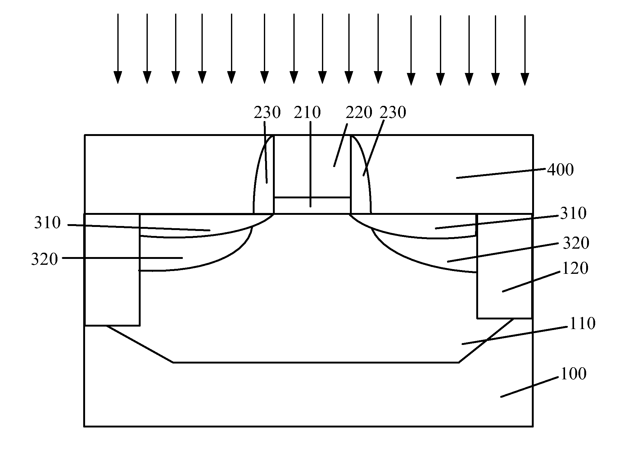
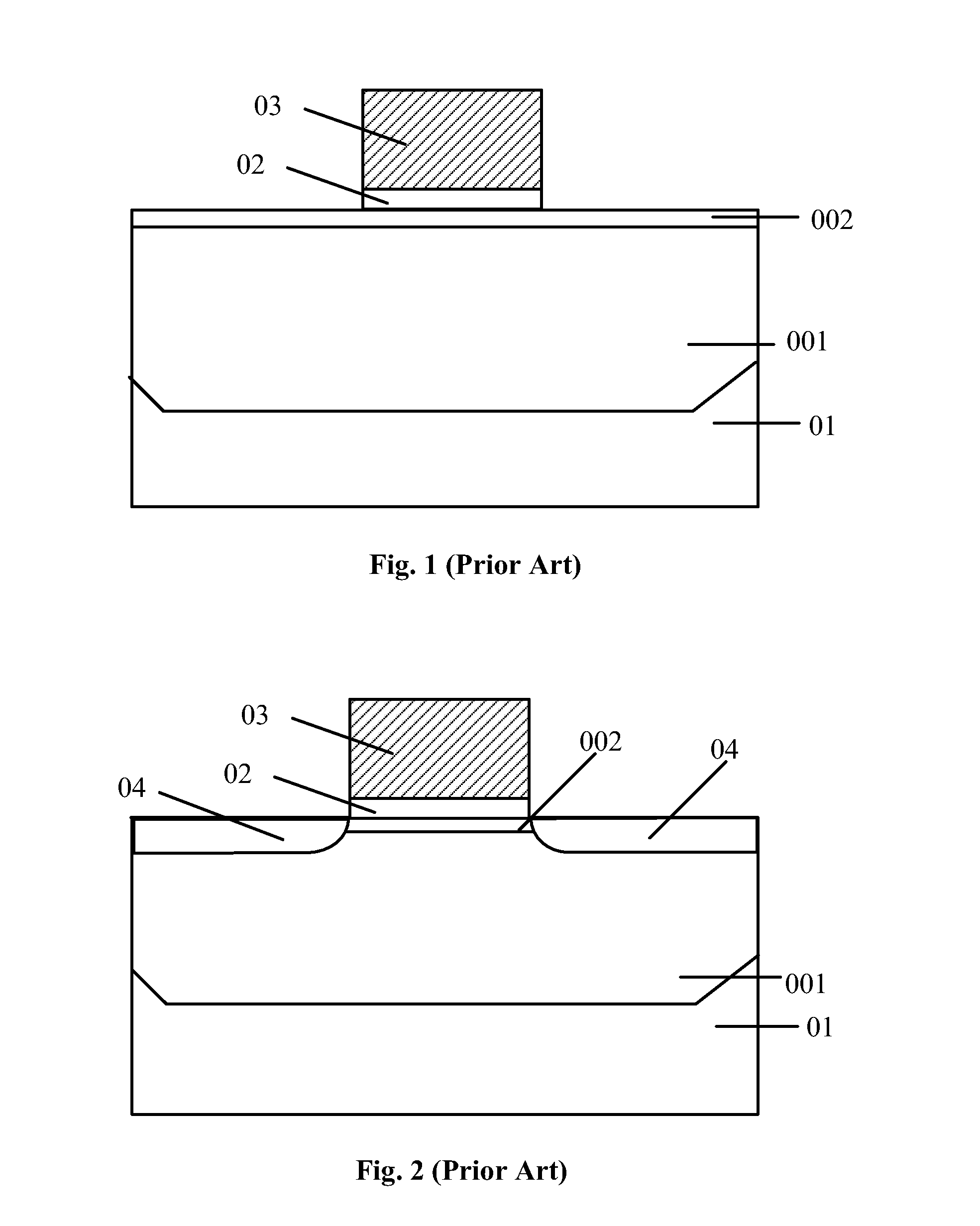
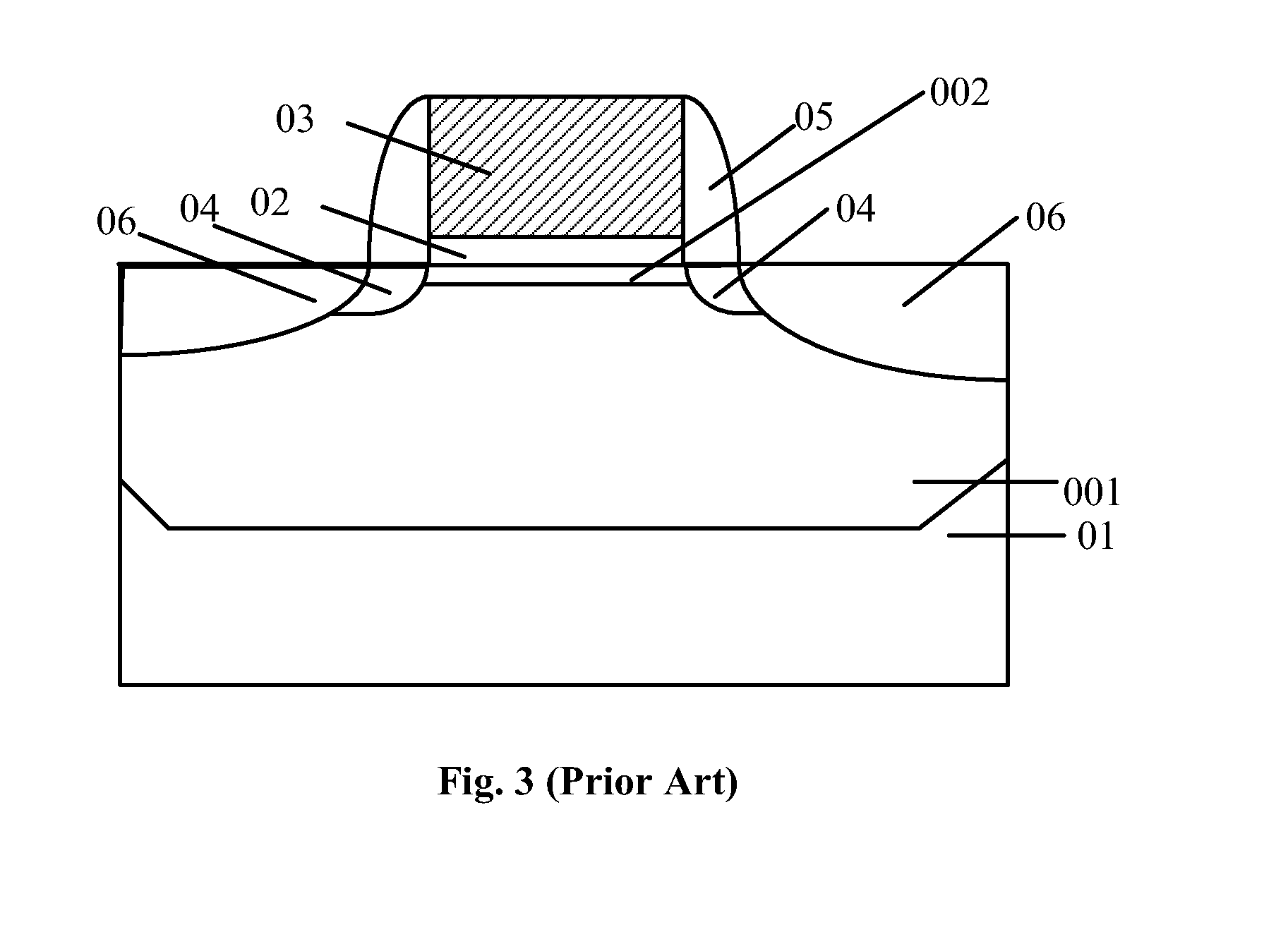
[0031]Inventor of the present invention had conducted numerous experiments and measurements, and discovered that ions (dopants) for adjusting the threshold voltage only need to be distributed in a portion of the substrate which is under the gate oxide layer and close to the surface of the substrate. However, in the prior art, the ions for adjusting the threshold voltage are implanted prior to forming the gate structure and forming the source / drain (S / D) regions. Those conventional methods require processes operating in high temperature environments or heat treatments, which may enhance the diffusion of the ions for adjusting the threshold voltage, make the ions diffuse deeper into the internal part of the substrate, enlarge the junction capacitance between the source / drain regions and the substrate, increase the junction leaking current, therefore lowers the operation speed and the performance of the transistor.

[0032]In order to solve these problems, an embodiment of the present inv...


PUM


Abstract

A method for forming a transistor includes providing a substrate, forming a well region in the substrate, and forming a gate structure on a surface of the well region. The gate structure includes a gate oxide layer on the surface of the well region and a gate on the gate oxide layer. The method further includes forming source/drain regions in the substrate at opposite sides of the gate structure and performing an ion doping to the substrate to adjust a threshold voltage. The ion doping is performed after the source/drain regions are formed to reduce the impact to the diffusion of the ions caused by heat treatments performed before the ion doping. The method further includes heating the substrate after the ion doping at a temperature from about 400° C. to about 500° C.

Description

CROSS-REFERENCES TO RELATED APPLICATIONS[0001]The present application claims the priority of Chinese Patent Application No. 201110136713.7, entitled “METHOD FOR FORMING A TRANSISTOR”, filed on May 25, 2011, the entire disclosure of which is incorporated herein by reference.FIELD OF THE INVENTION[0002]The present invention generally relates to the semiconductor field, and more particularly, to a method for forming a transistor having lower junction capacitance and improved switching performance.BACKGROUND OF THE INVENTION[0003]Metal-Oxide-Semiconductor (MOS) transistors are the most fundamental devices in semiconductor manufacturing processes and are widely used in various integrated circuits. MOS transistors are divided into NMOS transistors and PMOS transistors according to the major carriers and doping types thereof.[0004]FIGS. 1 to 3 are schematic cross-sectional views of intermediate structures of a conventional method for forming a MOS transistor.[0005]Referring to FIG. 1, a su...

Claims


Application Information

Patent Timeline
IPC IPC(8): H01L21/336
CPCH01L21/2652H01L29/6659H01L29/66545H01L29/66537
Inventor ZHAO, MENG
Owner SEMICON MFG INT (SHANGHAI) CORP
Why Eureka
Try Eureka