Computational Process Control

a process control and computation technology, applied in numerical control, electric digital data processing, instruments, etc., can solve the problems of insufficient independent optimization and difficulty in reproducing patterns on wafers, and achieve the performance stability of lithography apparatus/process, optimize process windows, and improve yield

Active Publication Date: 2012-11-29
ASML NETHERLANDS BV
View PDF3 Cites 35 Cited by
  • Summary
  • Abstract
  • Description
  • Claims
  • Application Information

AI Technical Summary

Benefits of technology

[0013]The present invention provides a number of innovations in the area of computational process control (CPC). CPC offers unique diagnostic capability during chip manufacturing cycle by analyzing temporal drift of a lithography apparatus / process, and provides a solution towards achieving performance stability of the lithography apparatus / process. Embodiments of the present invention enable optimized process windows and higher yields by keeping performance of a lithography apparatus and / or parameters of a lithography process substantially close to a pre-defined baseline condition. This is done by comparing the measured temporal drift to a baseline performance model. Once in manufacturing, CPC optimizes a scanner for specific patterns or reticles by leveraging wafer metrology techniques and feedback loop, and monitors and controls, among other things, overlay and / or CD uniformity (CDU) performance over time to continuously maintain the system close to the baseline condition. CPC can be tailored to a specific customer requirement, specific technology node, and / or specific application.

Problems solved by technology

These rules are set by processing and design limitations.
In general, the smaller k1 the more difficult it becomes to reproduce a pattern on the wafer that resembles the shape and dimensions planned by a circuit designer in order to achieve particular electrical functionality and performance.
However, migrating to 32-nm technology node and smaller, independent optimization is no longer enough.

Method used


Image

  • Computational Process Control
  • Computational Process Control
  • Computational Process Control

Examples


Embodiment Construction

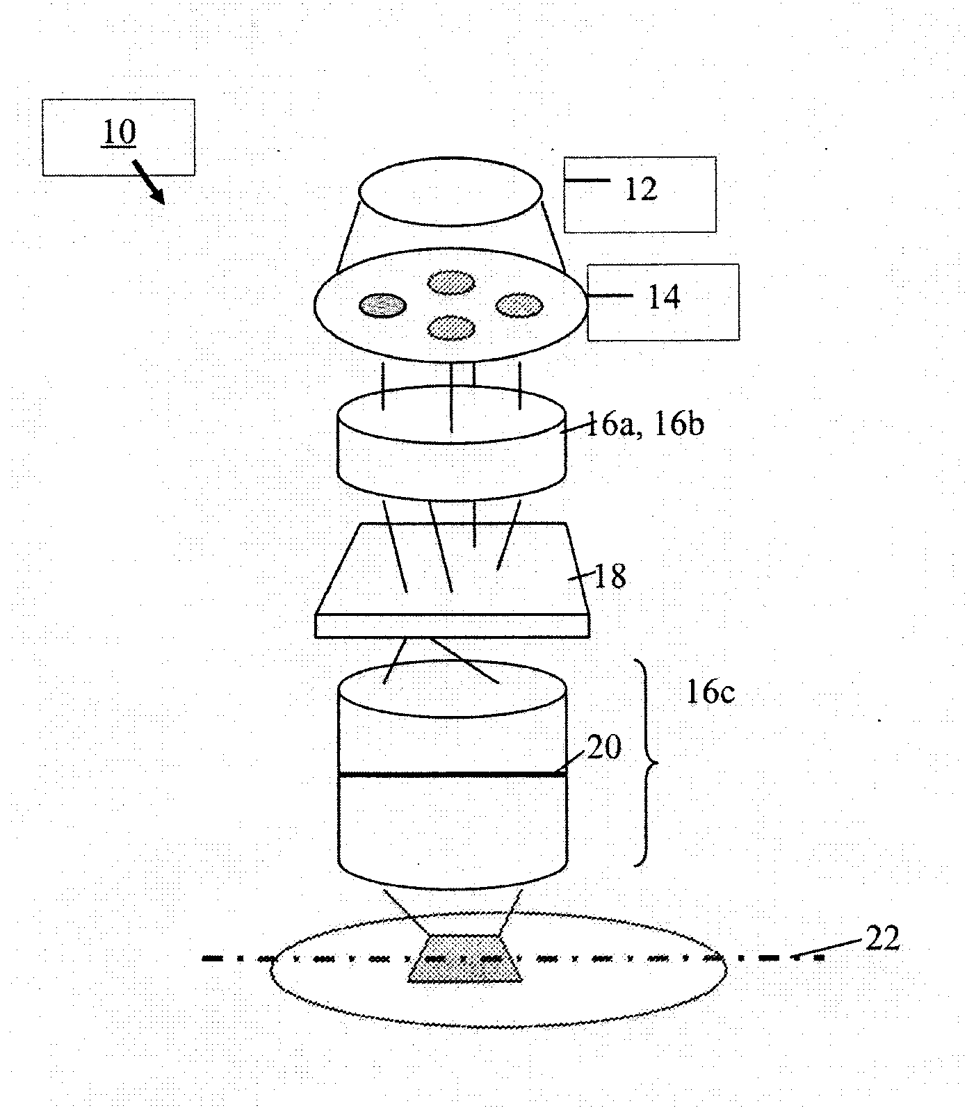
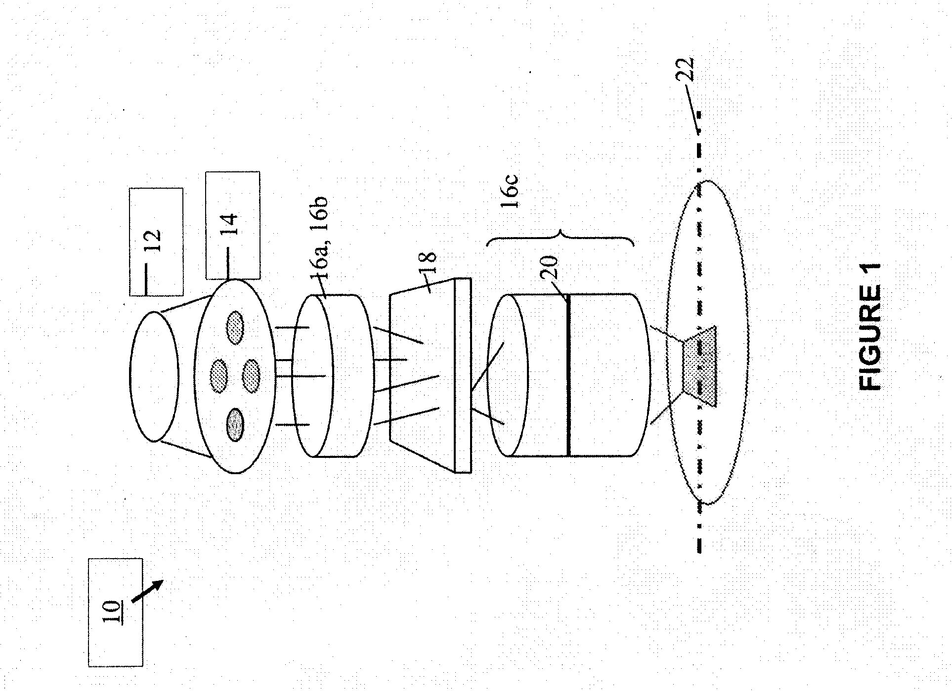
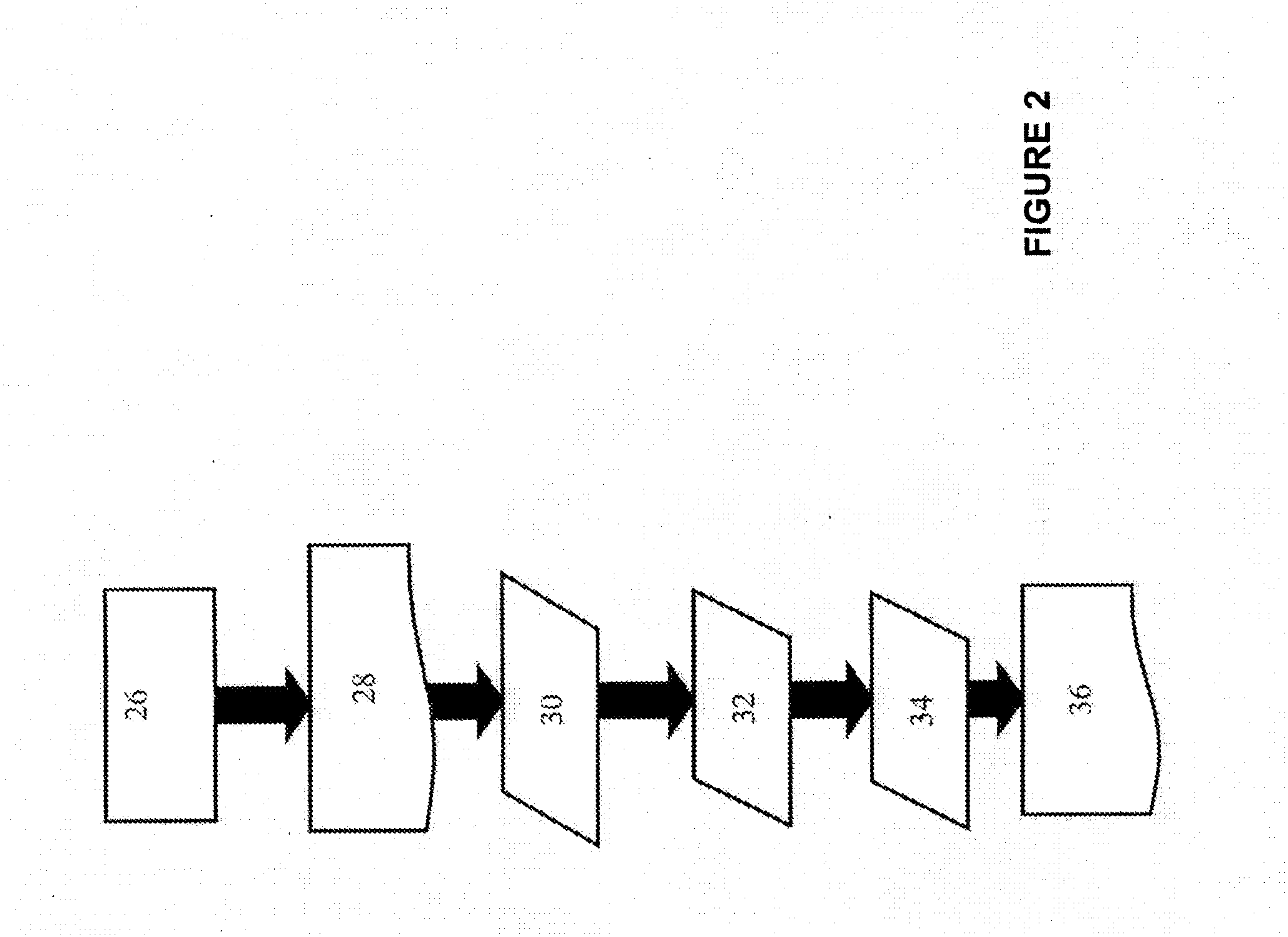
[0025]The present invention will now be described in detail with reference to the drawings, which are provided as illustrative examples of the invention so as to enable those skilled in the art to practice the invention. Notably, the figures and examples below are not meant to limit the scope of the present invention to a single embodiment, but other embodiments are possible by way of interchange of some or all of the described or illustrated elements. Moreover, where certain elements of the present invention can be partially or fully implemented using known components, only those portions of such known components that are necessary for an understanding of the present invention will be described, and detailed descriptions of other portions of such known components will be omitted so as not to obscure the invention. Embodiments described as being implemented in software should not be limited thereto, but can include embodiments implemented in hardware, or combinations of software and...


PUM

PropertyMeasurementUnit
wavelengthaaaaaaaaaa

Abstract

The present invention provides a number of innovations in the area of computational process control (CPC). CPC offers unique diagnostic capability during chip manufacturing cycle by analyzing temporal drift of a lithography apparatus/ process, and provides a solution towards achieving performance stability of the lithography apparatus/process. Embodiments of the present invention enable optimized process windows and higher yields by keeping performance of a lithography apparatus and/or parameters of a lithography process substantially close to a pre-defined baseline condition. This is done by comparing the measured temporal drift to a baseline performance using a lithography process simulation model. Once in manufacturing, CPC optimizes a scanner for specific patterns or reticles by leveraging wafer metrology techniques and feedback loop, and monitors and controls, among other things, overlay and/or CD uniformity (CDU) performance over time to continuously maintain the system close to the baseline condition.

Description

CROSS-REFERENCE TO RELATED APPLICATIONS[0001]This application claims priority to U.S. Provisional Application No. 61 / 490,010 filed May 25, 2011, which is incorporated herein by reference in its entirety.FIELD OF INVENTION[0002]The technical field of the present invention relates generally to lithography processes and apparatuses, and more specifically to performance stability control of lithography apparatuses and processes.BACKGROUND[0003]Lithographic apparatuses can be used, for example, in the manufacture of integrated circuits (ICs). In such a case, the mask may contain a circuit pattern corresponding to an individual layer of the IC, and this pattern can be imaged onto a target portion (e.g. comprising one or more dies) on a substrate (silicon wafer) that has been coated with a layer of radiation-sensitive material (resist). In general, a single wafer will contain a whole network of adjacent target portions that are successively irradiated via the projection system, one at a ti...

Claims


Application Information

Patent Timeline
Patent Type & Authority Applications(United States)
IPC IPC(8): G05B19/18
CPCG05B13/04G03F9/7096B29C67/0088G03F7/70525B29C64/393
Inventor YE, JUNCAO, YUKOONMEN, JAMES PATRICK
Owner ASML NETHERLANDS BV
Why Eureka
Try Eureka