Silicon carbide semiconductor device and method for manufacturing same

a silicon carbide semiconductor and semiconductor technology, applied in the field a manufacturing method of silicon carbide semiconductor devices, can solve the problems of difficult to sufficiently reduce the on-resistance of mosfet, the impurity concentration in the silicon carbide becomes unnecessarily high, and the carriers flowing in the silicon carbide are more frequently scattered by impurities, so as to achieve the effect of reducing the on-resistan

Active Publication Date: 2012-12-06
SUMITOMO ELECTRIC IND LTD
View PDF0 Cites 14 Cited by
  • Summary
  • Abstract
  • Description
  • Claims
  • Application Information

AI Technical Summary

Benefits of technology

[0009]The present invention has been made to solve such a problem and has its object to provide a silicon carbide semicondu...

Problems solved by technology

This makes it difficult to sufficiently reduce the on-resistance of the MOSFET.
In other words, the impurity concentration in the silicon carbide becomes unnecessarily high, with...

Method used


Image

  • Silicon carbide semiconductor device and method for manufacturing same
  • Silicon carbide semiconductor device and method for manufacturing same
  • Silicon carbide semiconductor device and method for manufacturing same

Examples


first embodiment

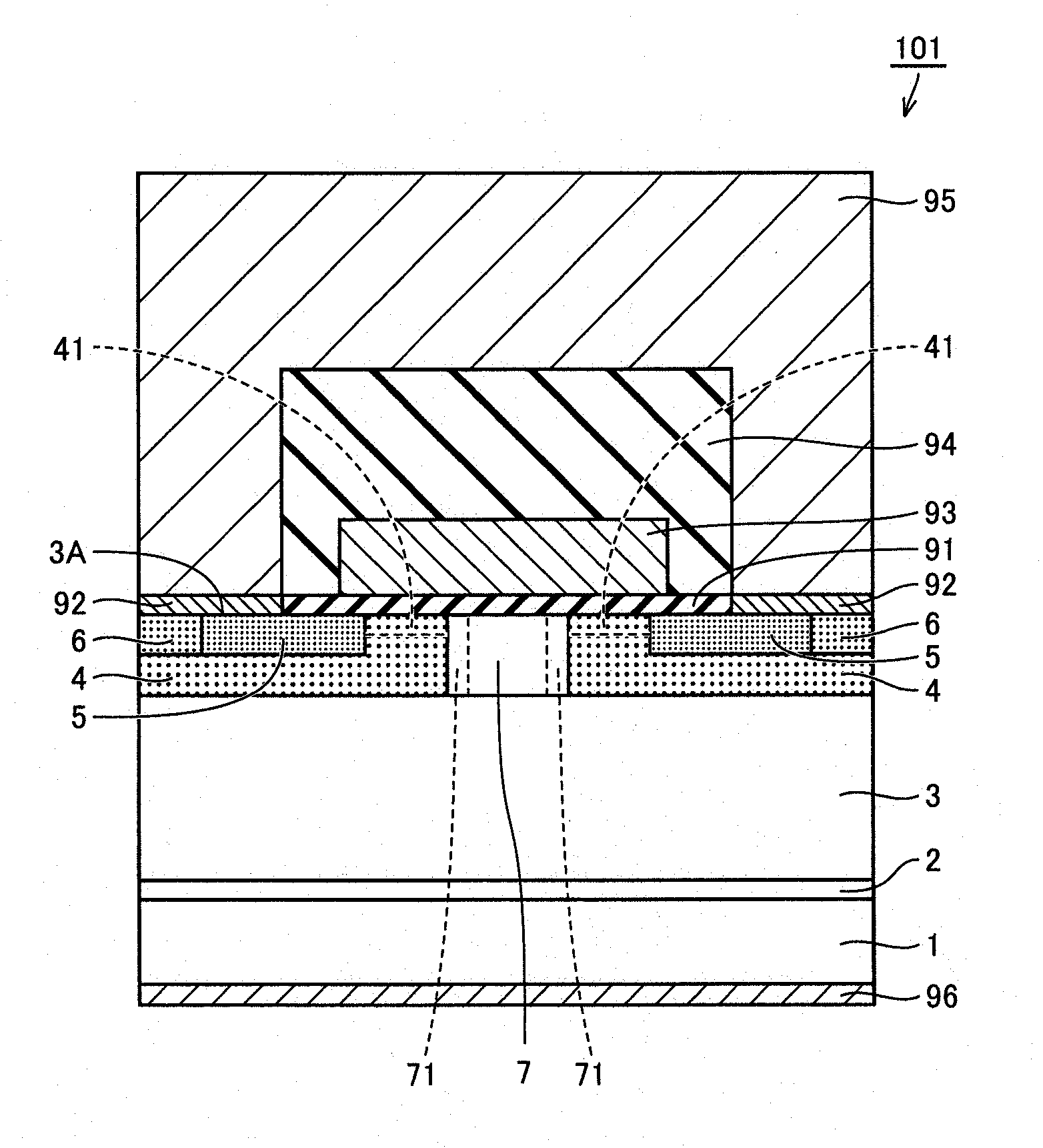
[0037]As shown in FIG. 1, a silicon carbide semiconductor device of the present embodiment is, in particular, a MOSFET 101 suitable for a power semiconductor device. More specifically, MOSFET 101 is a vertical type DiMOSFET (Double-Implanted MOSFET). MOSFET 101 includes a silicon carbide substrate 1, a buffer layer 2, a drift layer 3, a pair of body regions 4, n+ regions 5, p+ regions 6, a JFET region 7, a gate oxide film 91 (gate insulating film), source contact electrodes 92, a gate electrode 93, an interlayer insulating film 94, a source wire 95, and a drain electrode 96.

[0038]Drift layer 3 is provided over the upper surface of silicon carbide substrate 1 with buffer layer 2 interposed therebetween, and has a thickness direction (vertical direction in FIG. 1) throughout which a current flows. Further, drift layer 3 has an n type (first conductivity type) impurity concentration N1d. It should be noted that drift layer 3 has a p type (second conductivity type) impurity concentratio...

second embodiment

[0075]As shown in FIG. 6, instead of body regions 4, n+ regions 5, and p+ regions 6 of MOSFET 101 (FIG. 1), a MOSFET 102 of the present embodiment includes body regions 4v, n+ regions 5v, and p+ regions 6v. Further, each of body regions 4v has an n type impurity concentration N1b, which is different from that in the first embodiment in that N1b=N1j is not satisfied and N1b=N1d is satisfied instead. Specifically, the n type impurity concentration of body region 4v is substantially equal to the n type impurity concentration of drift layer 3. It should be noted that when a change of concentration profile in drift layer 3 is large, the concentration of a portion of drift layer 3 which faces body region 4v is regarded as a reference concentration.

[0076]Apart from the configuration described above, the configuration of the present embodiment is substantially the same as the configuration of the first embodiment. Hence, the same or corresponding elements are given the same reference charac...


PUM

PropertyMeasurementUnit
Thicknessaaaaaaaaaa
Electrical conductivityaaaaaaaaaa
Concentrationaaaaaaaaaa

Abstract

A drift layer has a thickness direction throughout which a current flows and has an impurity concentration N1d for a first conductivity type. A body region is provided on a portion of the drift layer, has a channel to be switched by a gate electrode, has an impurity concentration N1b for the first conductivity type, and has an impurity concentration N2b for the second conductivity type greater than the impurity concentration N1b. A JFET region is disposed adjacent to the body region on the drift layer, has an impurity concentration N1j for the first conductivity type, and has an impurity concentration N2j for the second conductivity type smaller than the impurity concentration N1j. N1j−N2j>N1d and N2j<N2b are satisfied.

Description

BACKGROUND OF THE INVENTION[0001]1. Field of the Invention[0002]The present invention relates to a silicon carbide semiconductor device and a method for manufacturing the silicon carbide semiconductor device.[0003]2. Description of the Background Art[0004]In recent years, there has been examined a method for manufacturing a vertical type MOSFET (Metal Oxide Semiconductor Field Effect Transistor) using silicon carbide.[0005]According to one method disclosed in Japanese Patent Laying-Open No 2009-158788 (Patent Literature 1), a substrate made of a semiconductor having a first conductivity type is first prepared. Onto the substrate, a material gas and a dopant gas of the first conductivity type are introduced to epitaxially grow a buffer layer thereon by means of vapor phase reaction. Onto the buffer layer, a material gas and a dopant gas of the first conductivity type are introduced to epitaxially grow a drift layer thereon by means of vapor phase reaction. Into a surface of the drift...

Claims


Application Information

Patent Timeline
IPC IPC(8): H01L29/161H01L21/334
CPCH01L29/0878H01L29/7802H01L29/66068H01L29/1095H01L29/66712
Inventor HONAGA, MISAKOMASUDA, TAKEYOSHIWADA, KEIJIHIYOSHI, TORU
Owner SUMITOMO ELECTRIC IND LTD
Why Eureka
Try Eureka