Method of manufacturing semiconductor device

a manufacturing method and semiconductor technology, applied in semiconductor devices, semiconductor/solid-state device details, electrical devices, etc., can solve the problems of poor chemical resistance of insulating film formed in this method, damage to the chip, and danger of the destruction of semiconductor elements, so as to increase the mechanical strength and increase the yield of production

Inactive Publication Date: 2012-12-13
PS4 LUXCO SARL
View PDF16 Cites 28 Cited by
  • Summary
  • Abstract
  • Description
  • Claims
  • Application Information

AI Technical Summary

Benefits of technology

[0023]According to embodiments of the invention, an insulating film, which is first formed inside the trench, is etched, and the trench is filled again with another insulating film, so that the insulating films inside the insulating ring form a two-stage structure including upper and lower stages. When one of the two stages of the insulating films has a seam due to deposition in the central portion of the trench in the width direction, the seam is capped by the stacked portion. This, consequently, prevents the substrate and the portion of inside the insulating ring from being separated in the shape of a column. That is, it is possible to prevent the portion of the substrate that is inside the insulating ring from being isolated. Therefore, since the portion (the TSV-forming portion) of the substrate inside the insulating ring does not move even if stress is applied to the TSV, for example, when stacking a chip, there is no danger that the interlayer insulating film is subjected to stress or the like. Consequently, mechanical strength is increased. As a result, according to the semiconductor device that has the insulating ring, which is manufactured by the method of the invention, it is possible to increase the yield of production.

Problems solved by technology

When the inventor has studied the foregoing method of forming the insulating ring, it was found that the following problems may cause.
This may cause damage to the chip, for example, by forming cracks 200.
When cracks reach a device region, there is a danger that the semiconductor elements may be destroyed (FIG. 4).
The method of forming the insulating ring, disclosed in JP2009-111061 A, is substantially the same, and may lead to problems that are substantially the same above.
However, the insulating film, which is formed in this method, has poor resistance to chemicals, and is greatly recessed due to being exposed to etching when a semiconductor element or the like is formed on the main surface of the substrate.
Thus, the flatness of the surface of the substrate may be damaged.
In addition, when the film is subjected to densification (thermal densification) in order to increase the resistance to etching, the volume of the SOD film or the like is greatly shrunk due to thermal densification, and in that case, the flatness is damaged.

Method used


Image

  • Method of manufacturing semiconductor device
  • Method of manufacturing semiconductor device
  • Method of manufacturing semiconductor device

Examples


first exemplary embodiment

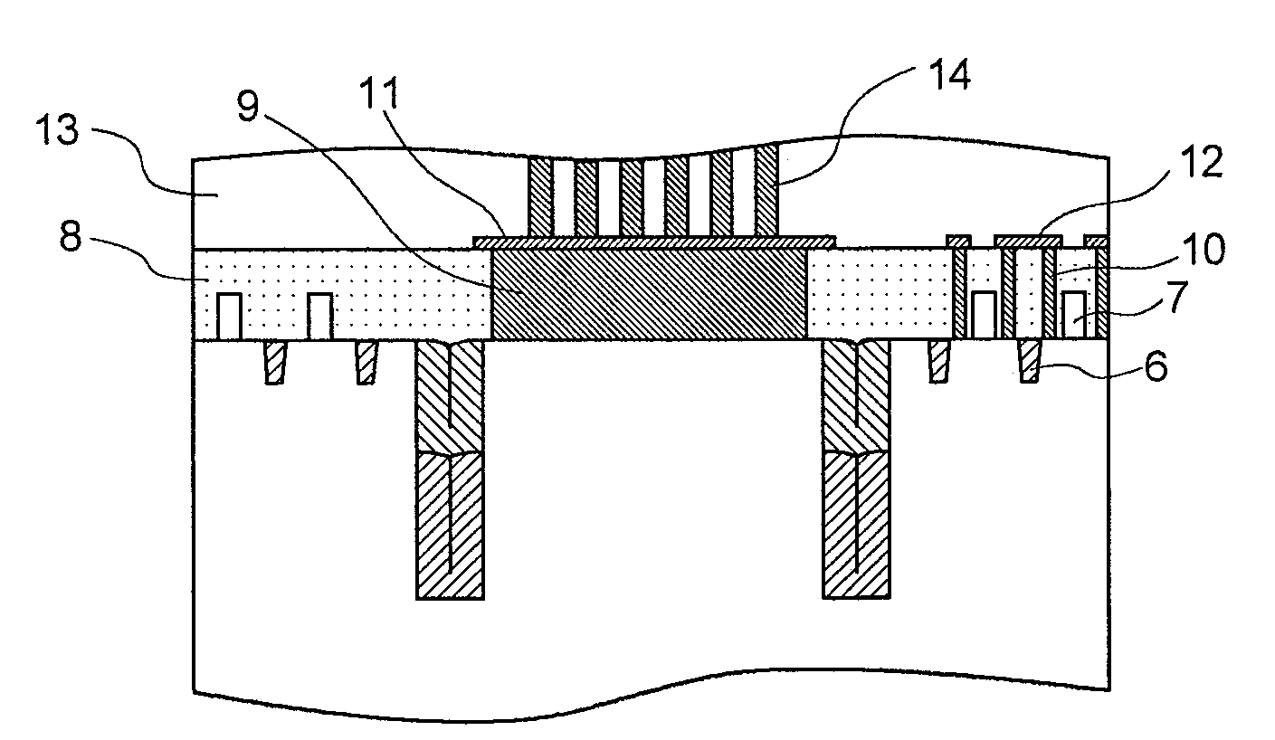
[0036]First, as shown in FIG. 6, a ring-shaped trench (a circular ring-shaped trench) 2 having a depth 50 μm and a width 2 μm is formed in a main surface side (first surface side) of a semiconductor substrate (silicon substrate) 1 by dry etching. The processing of the trench 2 includes forming a silicon nitride film (not shown) as a mask on the silicon substrate 1, and then the ring-shaped opening is formed using photolithography technology. In subsequence, the main surface of the silicon substrate 1 is selectively removed by etching using the shaped silicon nitride film as the mask. After the silicon substrate 1 is etched, the shaped silicon nitride film is removed. Alternatively, a next first insulating film may be formed without removing the shaped silicon nitride film.

[0037]In subsequence, a first insulating film 3 is deposited on the main surface of the silicon substrate 1, including the inside of the trench. Here, as the first insulating film 3, a non-doped silicate glass (NSG...

modified examples

[0053]In subsequence, modified examples of the first exemplary embodiment will be described.

[0054]In the foregoing explanation, both the first insulating film 3 and the second insulating film 4 are formed by CVD, as the films that have the seam 3S and the seam 4S, respectively. However, the invention is not limited to this construction, but one of the first and second insulating films can be formed by first deposition method, in which a seam is formed in the central portion of the width of the trench except for the bottom at the startup of the CVD, and the other insulating layer can be formed by second deposition method, in which no seam is formed. FIG. 13A shows the multi-stage structure including a first insulating film 3-1, which is formed by the first deposition method, and a second insulating film 4-2, which is formed by the second deposition method. In contrast, FIG. 13B shows the multi-stage structure including a first insulating film 3-2, which is formed by the second deposi...

second exemplary embodiment

[0062]In the first exemplary embodiment, etching back is performed after the first insulating film is formed. However, in some cases, the etching back is not necessary when the first insulating film is made of a flowable insulating material. FIG. 17A to FIG. 17D are process cross-sectional views depicting a method of manufacturing a semiconductor device, which includes a deposition process using a flowable insulating material by flowable CVD.

[0063]First, as shown in FIG. 17A, ring-shaped trenches 32a and 32b are formed in a silicon substrate 31 in order to form insulating rings. In this exemplary embodiment, a case, in which double insulating rings, including a first insulating ring and a second insulating ring, are formed, is presented. When the double insulating rings are formed, each width of the trenches is smaller than that of the trench of a single insulating ring, but the aspect ratio is increased due to the decreased trench width. A trench having a large aspect ratio tends t...


PUM


Abstract

The present invention provides a method of manufacturing a semiconductor device. An insulating-separating portion, which surrounds an electrode penetrating a substrate, is filled with a stacked structure of at least two stages, including a first stage of insulating film and a second stage of insulating film. When at least one of the first and second stages of insulating films has a seam, the seam is stopped by the region in the bottom of the second stage of insulating film that does not have a seam in at least the bottom thereof, thereby increasing mechanical strength. It is possible to prevent the inner region of the insulating-separating portion from being isolated.

Description

BACKGROUND OF THE INVENTION[0001]1. Field of the Invention[0002]The present invention relates to a method of manufacturing a semiconductor device, and more particularly, to a method of manufacturing a semiconductor device having an electrode that penetrates a semiconductor substrate.[0003]2. Related Art[0004]Recently, along with the high functionality and diversification of semiconductor devices, semiconductor devices that are integrated by stacking a plurality of semiconductor chips on each other in the lengthwise direction were proposed. Such a semiconductor device is configured such that electrical connection is established between the semiconductor chips using an electrode that penetrates a semiconductor substrate (so called a through silicon (or substrate) via: hereinafter abbreviated as “TSV”) of the semiconductor chips.[0005]Since the TSV is formed so as to penetrate the semiconductor substrate, it is necessary to provide insulation between the semiconductor substrate and the...

Claims


Application Information

Patent Timeline
Patent Type & Authority Applications(United States)
IPC IPC(8): H01L21/762
CPCH01L21/76898H01L23/481H01L21/76224H01L2924/0002H01L2924/00
Inventor KOBAYASHI, HIROTAKA
Owner PS4 LUXCO SARL
Why Eureka
Try Eureka