Powered grid for plasma chamber

Active Publication Date: 2012-12-20
LAM RES CORP
View PDF12 Cites 27 Cited by
  • Summary
  • Abstract
  • Description
  • Claims
  • Application Information

AI Technical Summary

Benefits of technology

[0014]Thus, as feature sizes continue to decrease to the low nanometer process nodes and beyond, it is no longer acceptable to experience drifts in etch equipment p

Problems solved by technology

The non-volatile reaction products, however, typically remain in the etching chamber in significant amounts.
Adherence of non-volatile reaction products to the window may interfere with the etching process.
Excessive deposition may result in particles flaking off the window onto the wafer, thus interfering with the etching process.
Excessive deposition, therefore, requires more frequent cleaning of the chamber walls and the window which adversely affects wafer throughput.
Additionally, if the window becomes coated with etch byproducts that are electrically conductive, the ability of the chamber transmit sufficient magnetic flux to the plasma becomes diminished, which in turn reduces the ability to control the directionality of etch operations, which are critical when processing high aspect ra

Method used


Image

  • Powered grid for plasma chamber
  • Powered grid for plasma chamber
  • Powered grid for plasma chamber

Examples


Embodiment Construction

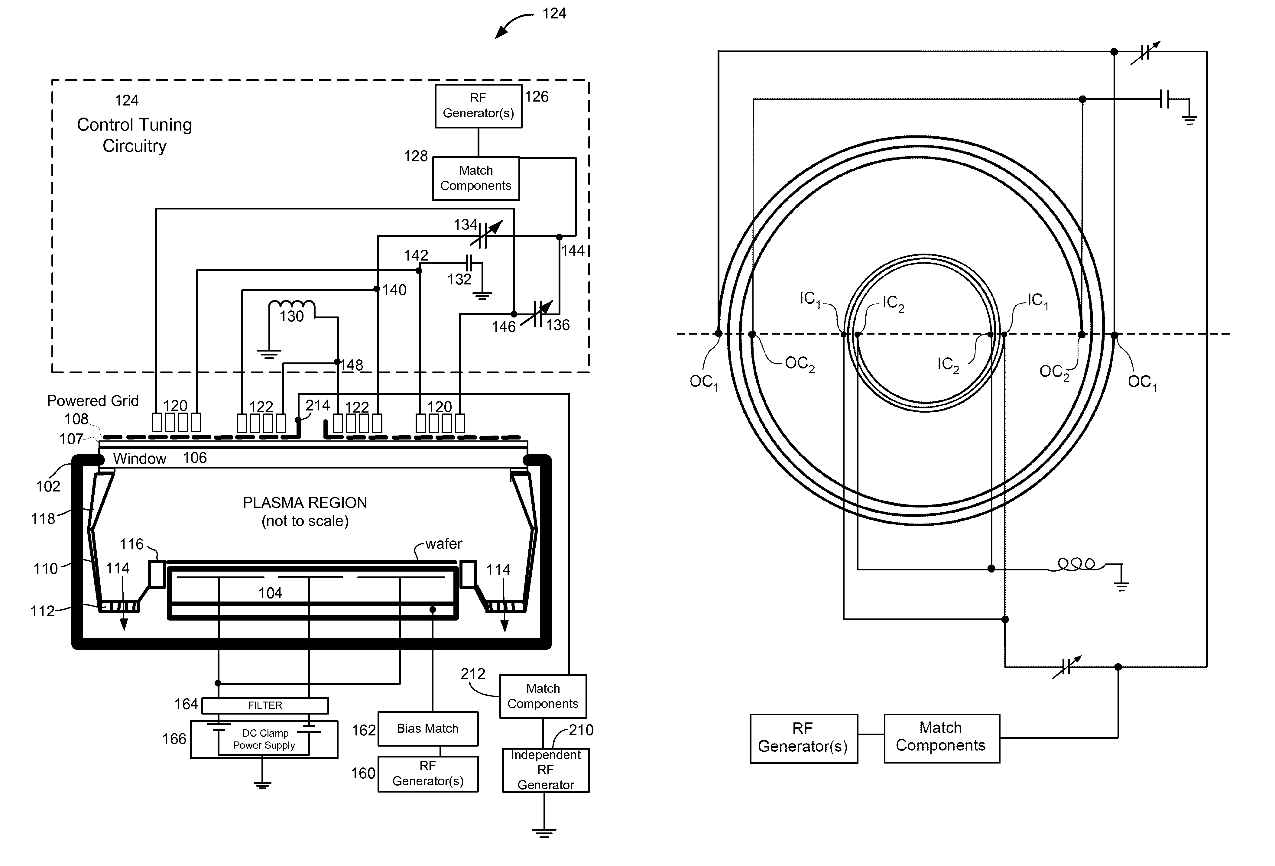
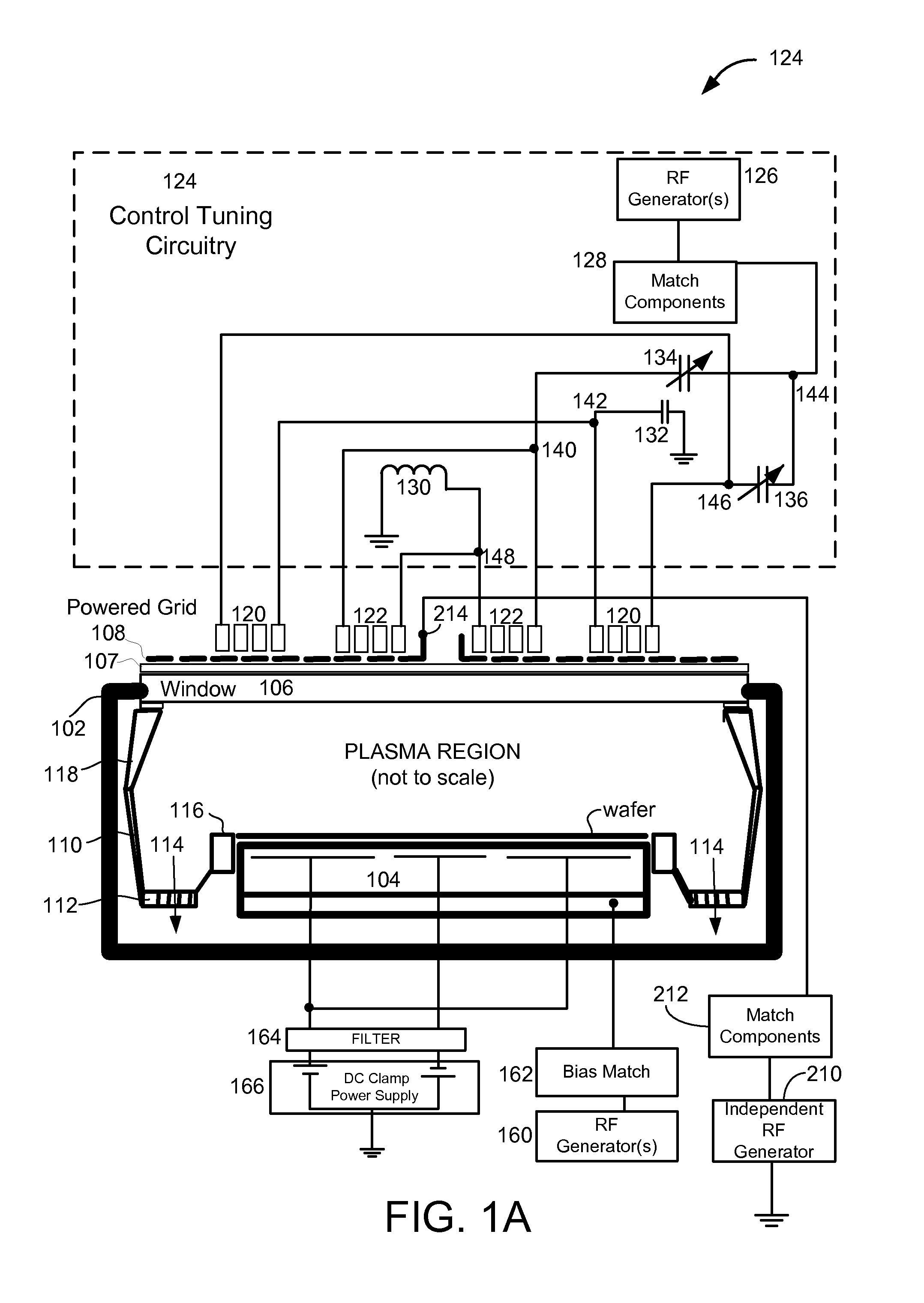
[0025]Disclosed is an apparatus used in etching semiconductor substrates and layers formed thereon during the manufacture of semiconductor devices. The apparatus is defined by a chamber in which etching is performed. A TCP coil is disposed over a dielectric window of the chamber, and a powered grid is disposed between dielectric window and the TCP coil. The powered grid is powered separately and independently of the power provided to the TCP coil. In the following description, numerous specific details are set forth in order to provide a thorough understanding of the present invention. However, it will be apparent to one skilled in the art that the present invention may be practiced without some of these specific details. In other instances, well known process operations and implementation details have not been described in detail in order to avoid unnecessarily obscuring the invention.

[0026]Due to the increasing demand for nonvolatile random access memory with long-term data retent...


PUM

PropertyMeasurementUnit
Frequencyaaaaaaaaaa
Frequencyaaaaaaaaaa
Frequencyaaaaaaaaaa

Abstract

A plasma processing chamber and methods for operating the chamber are provided. An exemplary chamber includes an electrostatic chuck for receiving a substrate and a dielectric window connected to a top portion of the chamber. An inner side of dielectric window faces a plasma processing region that is above the electrostatic chuck and an outer side of the dielectric window is exterior to the plasma processing region. Inner and outer coils are disposed above the outer side of the dielectric window, and the inner and outer coils are connected to a first RF power source. A powered grid is disposed between the outer side of dielectric window and the inner and outer coils. The powered grid is connected to a second RF power source that is independent from the first RF power source.

Description

1. FIELD OF THE INVENTION[0001]The present invention relates generally to semiconductor fabrication, and more particularly, to an apparatus containing a powered grid for maintaining the condition of a window of an inductively coupled plasma etching apparatus.2. DESCRIPTION OF THE RELATED ART[0002]In semiconductor manufacturing, etching processes are commonly and repeatedly carried out. As is well known to those skilled in the art, there are two types of etching processes: wet etching and dry etching. One type of dry etching is plasma etching performed using an inductively coupled plasma etching apparatus.[0003]A plasma contains various types of radicals, electrons, as well as positive and negative ions. The chemical reactions of the various radicals, positive ions, and negative ions are used to etch features, surfaces and materials of a wafer. During the etching process, a chamber coil performs a function analogous to that of a primary coil in a transformer, while the plasma perform...

Claims


Application Information

Patent Timeline
IPC IPC(8): H01L21/3065C23F1/08
CPCH01J37/321H01J37/32651H01L21/6831H01J37/32697
Inventor LONG, MAOLINPATERSON, ALEXMARSH, RICHARDWU, YING
Owner LAM RES CORP
Why Eureka
Try Eureka