
Wafer level molded opto-couplers

Inactive Publication Date: 2012-12-27
SEMICON COMPONENTS IND LLC
View PDF3 Cites 35 Cited by
  • Summary
  • Abstract
  • Description
  • Claims
  • Application Information

AI Technical Summary

Benefits of technology

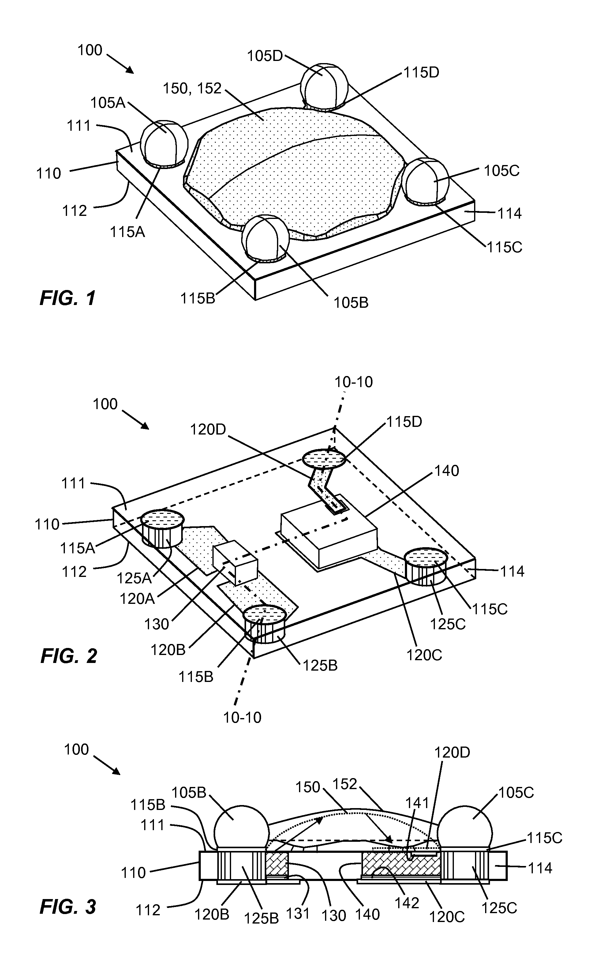
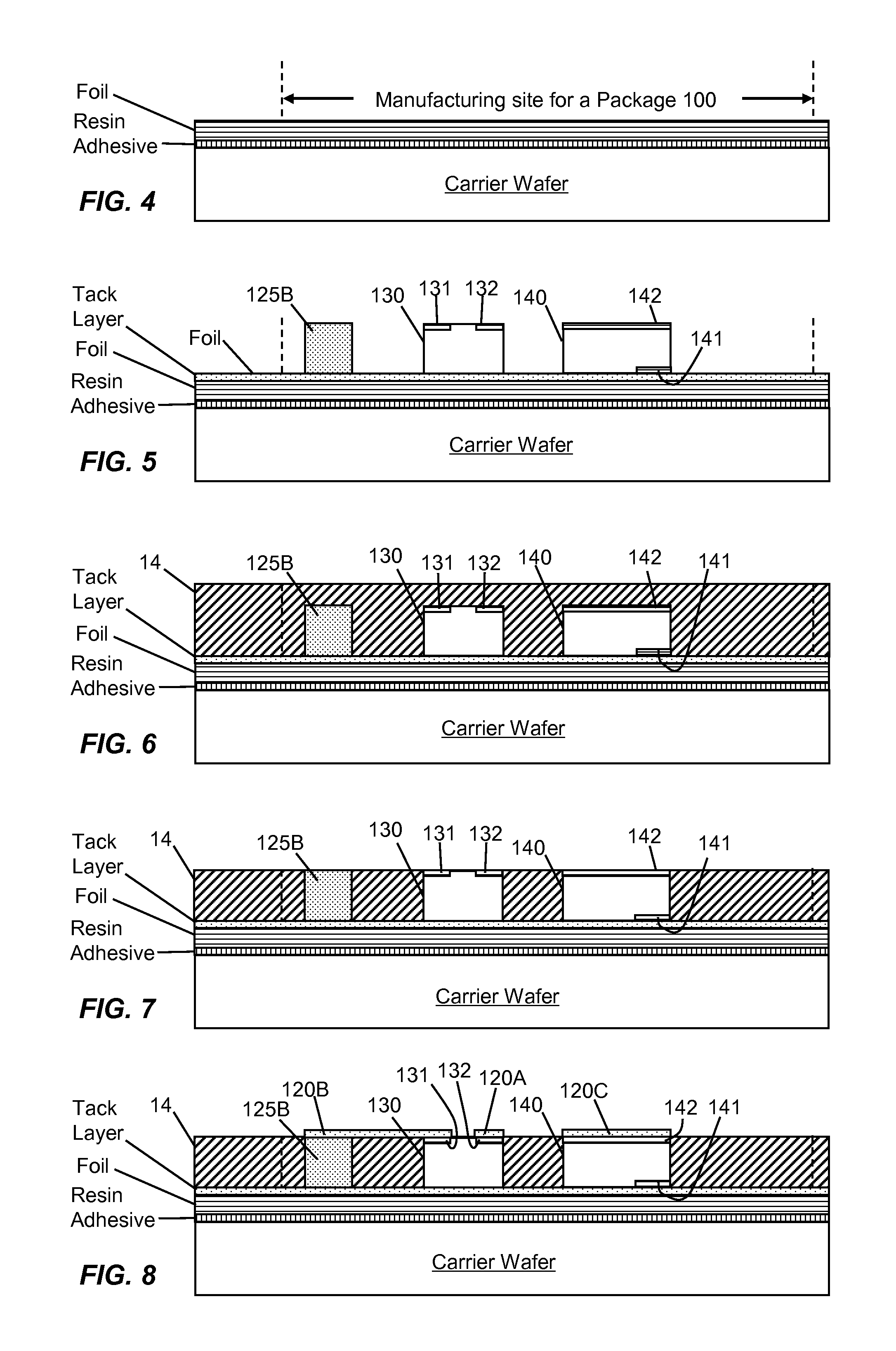
[0003]As part of making their invention, the inventors have recognized that optocouplers are being used in greater numbers in power conversion circuits, and that the relatively bulky size of multiple optocouplers in a power conversion circuit will be an impediment to allowing the size and volume of the circuit to be reduced. Also as part of making their invention, the inventors have recognized that there is a need to reduce the costs of optocouplers and to increase their electrical performance. Aspects of the present invention provide optocouplers with optoelectronic components embedded within a support substrate, and one or more ultra thin interconnect layers, which each provide for an ultra thin and ultra-small optocoupler package. The construction enables the support substrate and embedded components to be manufactured with a wafer-level molding and manufacturing processes in which multiple instances of the package are manufacture together on a common wafer using a common molding process and conventional semiconductor processes, and separated from the common wafer and one another after fabrication. This wafer-level manufacture approach can be automated to a high degree, which significantly lowers manufacturing costs. Further aspects of the present invention reduce manufacturing costs and improve electrical performance.
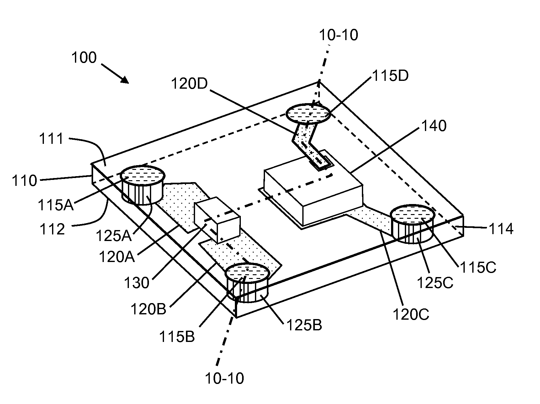
[0006]The above exemplary construction has many advantages. First, embedding the optoelectronic devices into the substrate reduces the thickness of package compared to prior art optocouplers where the optoelectronic devices are mounted on the surface of a substrate. Since the devices are embedded in the substrate, the body radiation transmissive material does need to encase the devices, and therefore can have a smaller height and smaller foot print area, thereby reducing the foot print area of the package. Also, the construction enables the traces to replace the wire bonds used in conventional optocoupler packages, which also reduces the height and foot print area of the packages. The elimination of wire bonds also increases the reliability of the package, enables wafer-level manufacturing processes to be used. Wafer-level processing allows for a high degree of automation, and generally results in lower costs compared to conventional lead frame methods. The smaller foot print of the package also enables a larger number of packages to be formed on a common wafer.

Problems solved by technology

First, embedding the optoelectronic devices into the substrate reduces the thickness of package compared to prior art optocouplers where the optoelectronic devices are mounted on the surface of a substrate.

Method used


Image

  • Wafer level molded opto-couplers
  • Wafer level molded opto-couplers
  • Wafer level molded opto-couplers

Examples


Embodiment Construction

[0013]The present invention will be described more fully hereinafter with reference to the accompanying drawings, in which exemplary embodiments of the invention are shown. This invention may, however, be embodied in different forms and should not be construed as limited to the embodiments set forth herein. Rather, these embodiments are provided so that this disclosure is thorough and complete and fully conveys the scope of the invention to one skilled in the art. In the drawings, the thicknesses of layers and regions may be exaggerated for clarity. The same reference numerals are used to denote the same elements throughout the specification. The elements may have different interrelationships and different positions for different embodiments.

[0014]It will also be understood that when a layer is referred to as being “on” another layer or substrate, it can be directly on the other layer or substrate, or intervening layers may also be present. It will also be understood that when an el...


PUM


Abstract

Optocoupler packages and methods of making the same. An exemplary package comprises a substrate having a first surface, a second surface opposite the first surface, and a body of electrically insulating material disposed between the first and second surfaces; a first optoelectronic device embedded in the body of electrically insulating material of the substrate and disposed between the substrate's first and second surfaces, the first optoelectronic device having a first conductive region and a second conductive region; a second optoelectronic device embedded in the body of electrically insulating material of the substrate and disposed between the substrate's first and second surfaces and optically coupled to the first optoelectronic device, the second optoelectronic device having a first conductive region and a second conductive region; and a plurality of electrical traces disposed on one or both surfaces of the substrate and electrically coupled to the conductive regions of the optoelectronic devices.

Description

CROSS-REFERENCES TO RELATED APPLICATIONS[0001]None.BACKGROUND OF THE INVENTION[0002]An optocoupler contains an optical emitter device that is optically coupled to an optical receiver device through an optically transmissive material. This arrangement permits the passage of information from one electrical circuit that contains the optical emitter device to another electrical circuit that contains the optical receiver device. A high degree of electrical isolation is maintained between the two circuits. Because information is passed optically across an electrically insulating gap, the transfer is one way. For example, the optical receiver device cannot modify the operation of a circuit containing the optical emitter device. This feature is desirable because, for example, the emitter may be driven by a low voltage circuit using a microprocessor or logic gates, while the output optical receiver device may be part of a high voltage DC or AC load circuit. The optical isolation also prevent...

Claims


Application Information

Patent Timeline
IPC IPC(8): H01L33/48H01L33/62
CPCH01L25/167H01L24/18H01L2924/12041H01L2924/00H01L2924/12042H01L2924/12043H01L21/568H01L24/24H01L24/25H01L24/82H01L2224/04105H01L2224/12105H01L2224/2518
Inventor LIU, YONGQIAN, QIUXIAO
Owner SEMICON COMPONENTS IND LLC
Learn More