Composite material, light-emitting element, light-emitting device, electronic device, lighting device, and organic compound

a technology of light-emitting elements and composite materials, which is applied in the direction of oxide conductors, conductors, non-metal conductors, etc., can solve the problems of low transmittance, inability to efficiently extract light generated within the element, and inability to achieve efficient extraction of light, etc., to achieve excellent carrier injection properties, high visible light-transmitting properties, and high transport properties

Active Publication Date: 2013-01-10
SEMICON ENERGY LAB CO LTD
View PDF7 Cites 11 Cited by
  • Summary
  • Abstract
  • Description
  • Claims
  • Application Information

AI Technical Summary

Benefits of technology

[0042]According to one embodiment of the present invention, it is possible to provide a composite material which includes an organic compound and an inorganic compound and has a high carrier-transport property. It is also possible to provide a composite material which has an excellent property of carrier injection to an organic compound. It is also possible to provide a composite material in which light absorption due to charge transfer interaction is unlikely to occur. It is also possible to provide a composite material which has a high visible-light-transmitting property.
[0043]According to one embodiment of the present invention, it is possible to provide a light-emitting element which has high emission efficiency by application of the above composite material to the light-emitting element. It is also possible to provide a light-emitting element with low driving voltage. It is also possible to provide a light-emitting element with a long lifetime. It is possible to provide a light-emitting device including the light-emitting element, an electronic device including the light-emitting device, or a lighting device including the light-emitting device.

Problems solved by technology

However, as described in the Non-Patent Document 1, PANI has a problem that transmittance becomes lower when a film thickness becomes thick.
In other words, the problem lies in the transparency of the material itself that is used for the buffer layer; thus, light generated within the element cannot be extracted efficiently.
However, as apparent from an embodiment, for the mixed layer of an organic compound and a metal oxide that is disclosed in Patent Document 1, a high absorption peak is observed not only in the infrared region but also in the visible light region (around 500 nm), and a problem in transparency occurs.
Therefore, as expected, light generated within the element cannot be extracted efficiently, and the light emission efficiency of the element is degraded.

Method used


Image

  • Composite material, light-emitting element, light-emitting device, electronic device, lighting device, and organic compound
  • Composite material, light-emitting element, light-emitting device, electronic device, lighting device, and organic compound
  • Composite material, light-emitting element, light-emitting device, electronic device, lighting device, and organic compound

Examples


embodiment 1

[0091]In this embodiment, a composite material of one embodiment of the present invention will be described.

[0092]A composite material of one embodiment of the present invention is a composite material of an organic compound having a particular skeleton and an inorganic compound. There is no limitation on a method of preparing the composite material of one embodiment of the present invention; for example, it can be formed by a co-evaporation method in which the organic compound and the inorganic compound are deposited at the same time. The mixing ratio, in mass ratio, of the organic compound to the inorganic compound in the composite material of one embodiment of the present invention is preferably approximately 8:1 to 1:2 (=Organic compound: inorganic compound), and more desirably, 4:1 to 1:1 (=Organic compound: inorganic compound). When the composite material is formed by a co-evaporation method, the mixing ratio can be controlled by separately adjusting the deposition rates for t...

embodiment 2

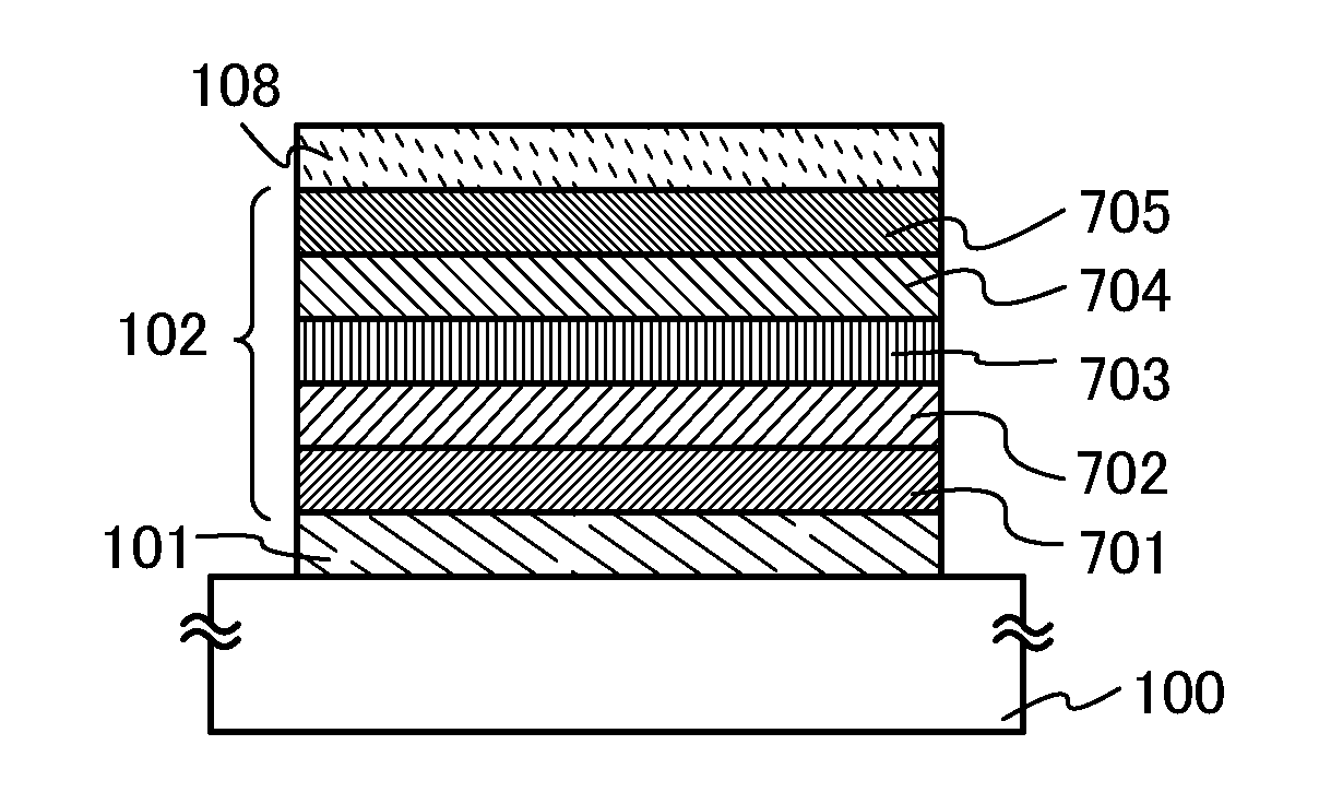
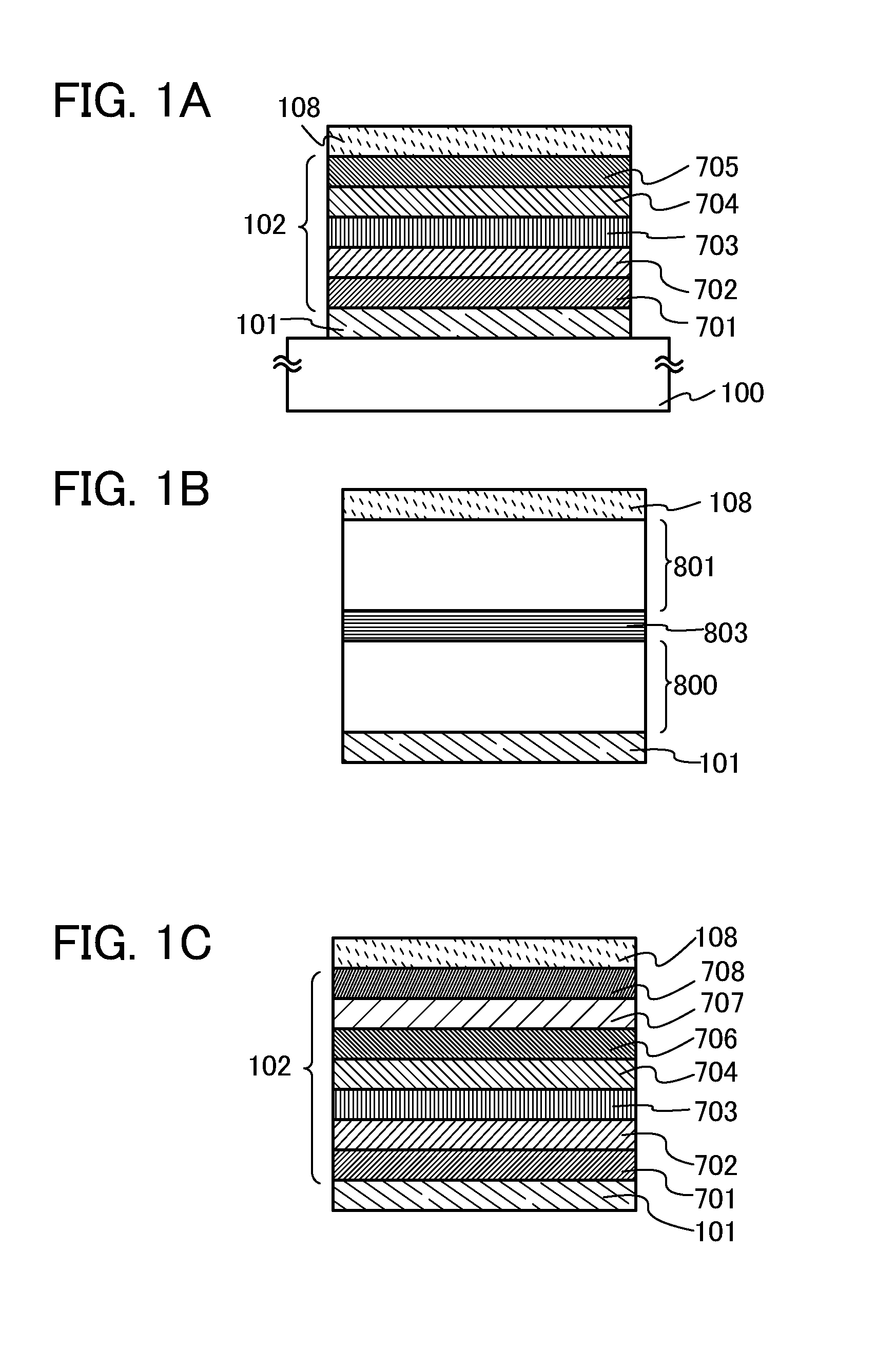
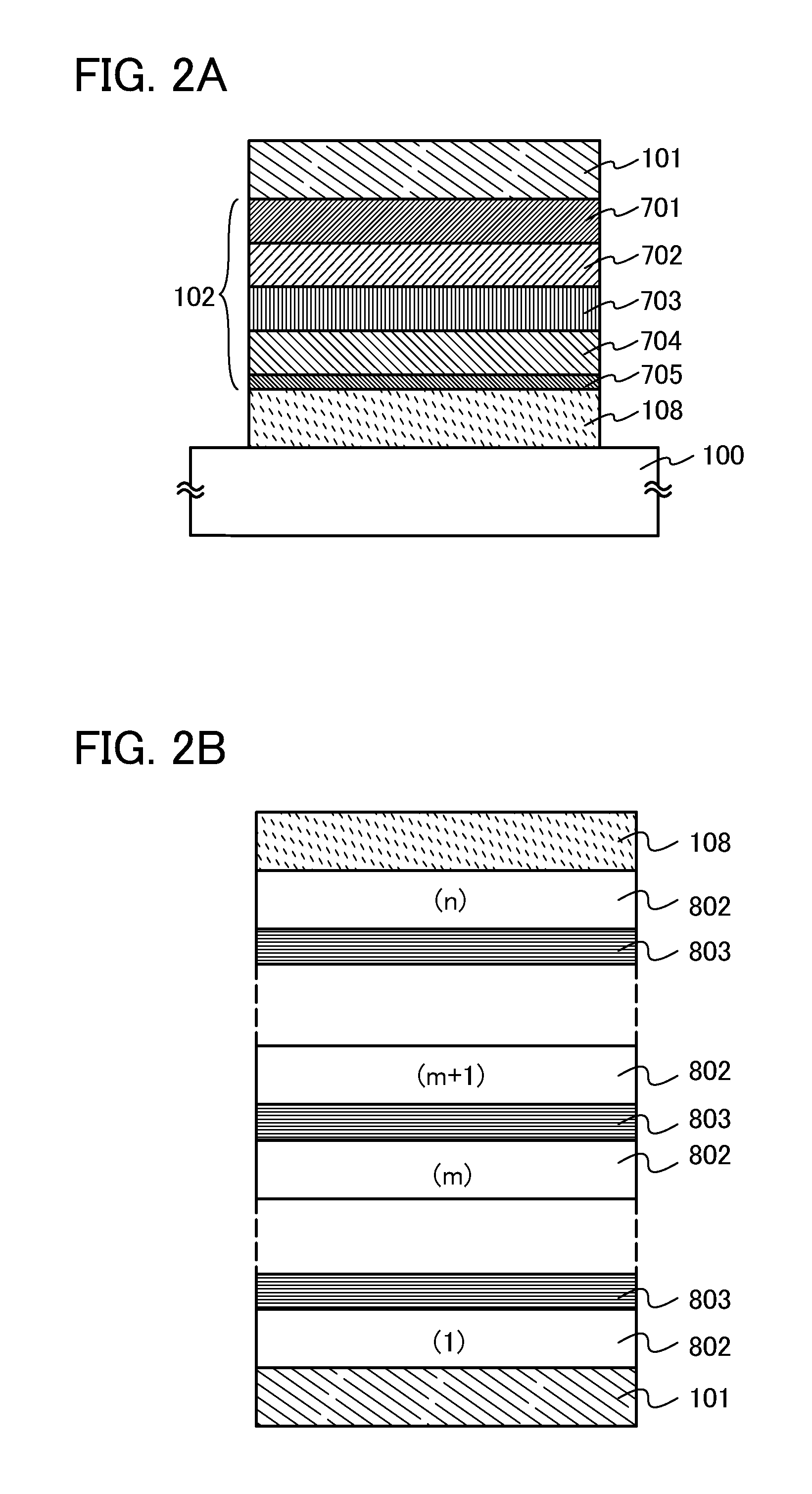
[0114]In this embodiment, a light-emitting element of one embodiment of the present invention will be described with reference to FIGS. 1A to 1C.

[0115]In a light-emitting element of this embodiment, an EL layer (a layer containing a light-emitting substance) is interposed between a pair of electrodes. The EL layer includes at least a layer containing the composite material of one embodiment of the present invention described in Embodiment 1 and a light-emitting layer. The EL layer may additionally include another layer. For example, the EL layer may include a layer containing a substance having a high carrier-injection property or a layer containing a substance having a high carrier-transport property so that a light-emitting region is formed in a region away from the electrodes, that is, so that carriers recombine in a region away from the electrodes. In this specification, the layer containing a substance having a high carrier-injection or a high carrier-transport property is also...

embodiment 3

[0175]In this embodiment, a light-emitting device including a light-emitting element of one embodiment of the present invention will be described with reference to FIGS. 3A and 3B. FIG. 3A is a top view illustrating a light-emitting device. FIG. 3B is a cross-sectional view taken along lines A-B and C-D in FIG. 3A.

[0176]The light-emitting device of this embodiment includes a source side driver circuit 401 and a gate side driver circuit 403 which are driver circuit portions, a pixel portion 402, a sealing substrate 404, a sealant 405, a flexible printed circuit (FPC) 409, and an element substrate 410. A portion enclosed by the sealant 405 is a space.

[0177]Note that a lead wiring 408 is a wiring for transmitting signals that are to be inputted to the source driver circuit 401 and the gate driver circuit 403, and receives a video signal, a clock signal, a start signal, a reset signal, and the like from an FPC 409 which serves as an external input terminal. Although only the FPC is illu...


PUM

PropertyMeasurementUnit
transmittanceaaaaaaaaaa
visible-light wavelengthsaaaaaaaaaa
work functionaaaaaaaaaa

Abstract

A composite material including an organic compound and an inorganic compound, which has a high carrier-transport property; a composite material having an excellent property of carrier injection to an organic compound; a composite material in which light absorption due to charge transfer interaction is unlikely to occur; and a composite material having a high visible-light-transmitting property are provided. A composite material which includes an organic compound and an inorganic compound exhibiting an electron-accepting property with respect to the organic compound, in which the rings of the organic compound are all benzene rings and the number of the benzene rings of the organic compound is greater than or equal to 4 and less than or equal to 25, is provided.

Description

BACKGROUND OF THE INVENTION[0001]1. Field of the Invention[0002]The present invention relates to a composite material including an organic compound and an inorganic compound, a light-emitting element, a light-emitting device, an electronic device, and a lighting device. The present invention also relates to an organic compound that can be used for the composite material.[0003]2. Description of the Related Art[0004]In recent years, research and development have been extensively conducted on light-emitting elements using organic electroluminescence (EL). The light-emitting elements have a basic structure in which a layer containing a light-emitting organic compound is interposed between a pair of electrodes. By applying voltage to this element, light can be emitted from the light-emitting organic compound.[0005]Since such a light-emitting element is of self-light-emitting type, it is considered that the light-emitting element has advantages over a liquid crystal display in that visibi...

Claims


Application Information

Patent Timeline
Patent Type & Authority Applications(United States)
IPC IPC(8): H01B1/12H01B1/08C07F7/08H01L51/54
CPCC07F15/0033C07F7/0809H01L51/0052H01L51/5088H01L51/0085H01L51/0094H01L51/0072C07F7/0805H10K85/615H10K85/40H10K85/342H10K85/6572H10K50/17
Inventor SEO, HIROMIOSAKA, HARUESEO, SATOSHISUZUKI, MASATOOHSAWA, NOBUHARU
Owner SEMICON ENERGY LAB CO LTD
Why Eureka
Try Eureka