System and Method For Providing High Resolution Digital-To-Analog Conversion Using Low Resolution Digital-To-Analog Converters

Active Publication Date: 2013-01-17
RENESAS ELECTRONICS CORP
View PDF1 Cites 9 Cited by
  • Summary
  • Abstract
  • Description
  • Claims
  • Application Information

AI Technical Summary

Benefits of technology

[0015]That is, with improved resolution and reduced influence of an error in a circuit characteristic realized by a relatively simple configuration, DA conversion can be performed. More specifically, the influence of an error or the like in a nominal

Problems solved by technology

From the viewpoint of the gist of the examination, in the patent documents, errors to be correc

Method used


Image

  • System and Method For Providing High Resolution Digital-To-Analog Conversion Using Low Resolution Digital-To-Analog Converters
  • System and Method For Providing High Resolution Digital-To-Analog Conversion Using Low Resolution Digital-To-Analog Converters
  • System and Method For Providing High Resolution Digital-To-Analog Conversion Using Low Resolution Digital-To-Analog Converters

Examples


first embodiment

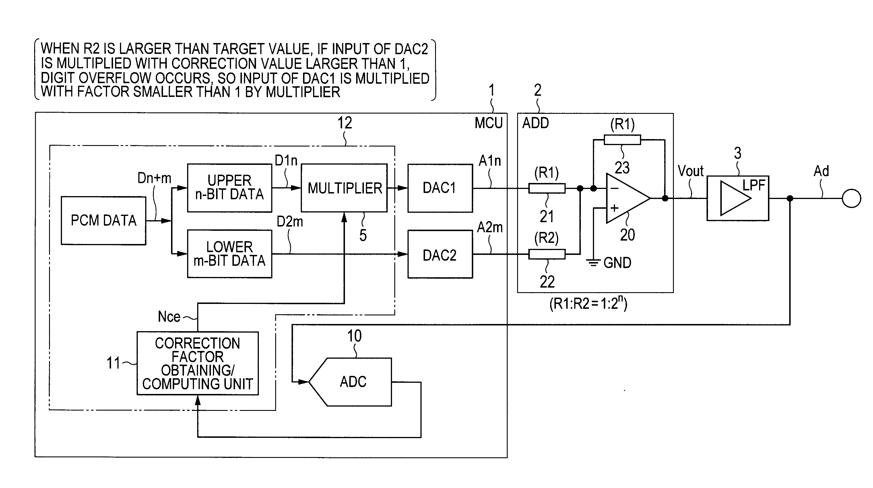
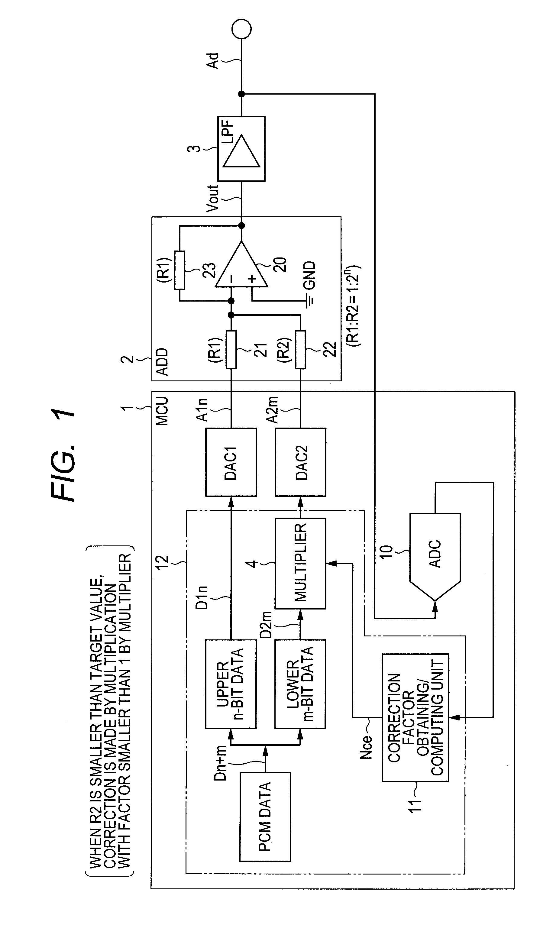
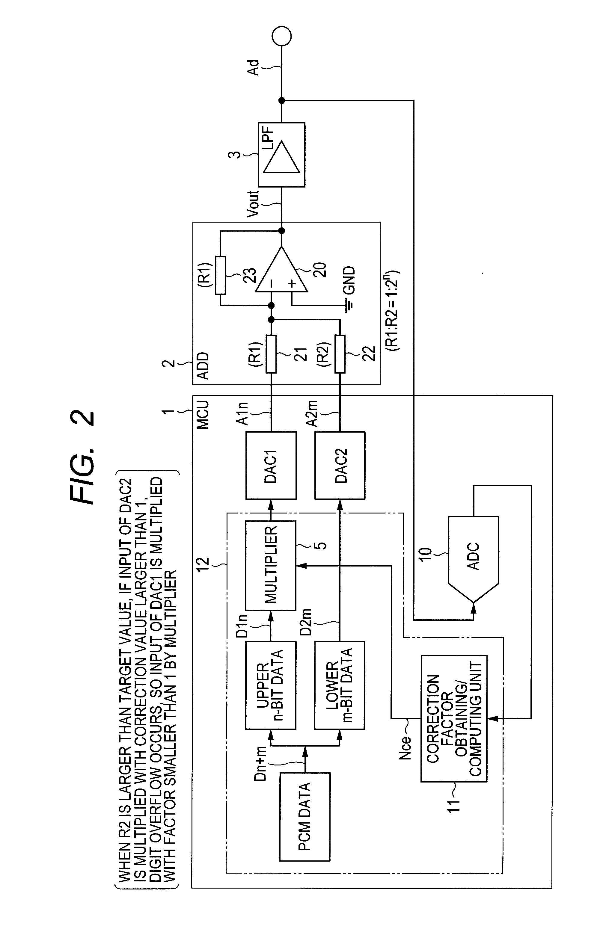
[0080]FIG. 1 illustrates a DA converting function realized by a data processing system as an embodiment of the present invention. The DA converting function shown in the diagram is a function of converting a digital signal having N bits, where N is greater than the individual resolution of any of DA converters DAC1 and DAC2 as on-chip elements of a microcomputer (MCU) 1 by using the plurality of DA converters DAC1 and DAC2. For example, a basic configuration is that PCM data Dn+m (comprised of n+m bits) to be subjected to digital process in the microcomputer (MCU) 1 is divided into upper n-bit data D1n and lower m-bit data D2m, the data D1n and D2m are converted to analog signals A1n and A2m by using the DA converters DAC1 and DAC2, respectively, and the analog signals A1n and A2m are added by an adder (ADD) 2 to generate a sound signal Ad via a low-pass filter 3.

[0081]The adder 2 adds the analog signal A2m to the analog signal A1n with a predetermined weight according to the resist...

second embodiment

[0100]FIG. 6 illustrates a data processing system 100 according to a second embodiment of the invention. The data processing system 100 shown in the diagram, although not so limited, performs temperature control according to a result of temperature measurement performed by a temperature sensor 30 and control vocal guidance based on the measurement result.

[0101]To the microcomputer 1, in addition to the adder 2 and the low-pass filter 3, a power amplifier 31 amplifying an output signal Ad of the low-pass filter 3 representatively shown and a speaker 32 receiving an output of the power amplifier 31 are coupled.

[0102]The microcomputer 1 is, although not limited, formed on a single semiconductor substrate made of single crystal silicon or the like by the known CMOS integrated circuit manufacturing technique or the like. The microcomputer 1 has a central processing unit (CPU) 41 and a program memory 42 storing an operation program of the CPU 41, each coupled as a program control circuit ...

third embodiment

[0112]FIG. 9 illustrates a data processing system 101 using a reconfigurable analog circuit. The main difference from the data processing system of FIG. 6 is that the adder 2 and the low-pass filter 3 are configured by using a reconfigurable analog circuit 8. The reconfigurable analog circuit 8 is a circuit in which a desired analog circuit function can be reconfigured by control data supplied to a control register 50 via the internal bus 40 under control of the CPU 41. Although not limited, in FIG. 9, the reconfigurable analog circuit 8 is configured as a semiconductor integrated circuit of one chip. The diagram shows a state where a function is set in the form of series connection of the adder 2 and the low-pass filter 3 by control data set in the control register 50. In FIGS. 1-4, the resistive elements 21, 22, and 23 coupled to the amplifier 20 as a component of the adder 2 are external elements. In the third embodiment, the reconfigurable analog circuit 8 and the microcomputer ...


PUM


Abstract

DA conversion is performed while improving resolution and reducing the influence of errors. A predetermined weight is applied to an output of at least one of a plurality of DA converters to each of which calibration data is given; the resultant outputs are added by an adder. An output of the adder is converted to a digital value by an AD converter. If the predetermined weight has an error outside an allowable range on the basis of the obtained digital value, a calibrating process of obtaining a correction factor for correcting the digital signal to be converted so as to reduce influence of the error is controlled. When a digital signal is to be converted to an analog signal with high precision, the digital signal is corrected with the correction factor, the resultant value is supplied to the DA converters, and DA converted outputs are added by the adder.

Description

CROSS-REFERENCE TO RELATED APPLICATIONS[0001]The disclosure of Japanese Patent Application No. 2011-154815 filed on Jul. 13, 2011 including the specification, drawings and abstract is incorporated herein by reference in its entirety.FIELD OF THE INVENTION[0002]The present invention relates to a digital-to-analog (“DA”) conversion technique for improving DA conversion precision using a plurality of DA converting circuits and, for example, relates to a technique effectively applied to a microcomputer system having a sound reproducing function of DA converting pulse-code modulation (“PCM”) data.BACKGROUND OF THE INVENTION[0003]There is a related technique of, using a plurality of DA converting circuits of low resolution such as eight bits provided in a microcomputer, realizing DA conversion of higher resolution.[0004]Japanese Patent No. 2000-278134 discloses a technique for performing high-resolution DA conversion. According to this technique, a digital signal is divided into upper bit...

Claims


Application Information

Patent Timeline
IPC IPC(8): H03M1/10H03M1/66
CPCH03M1/68H03M1/1061
Inventor ISO, YOSHIMIHIROSHIMA, AKANETAMAKI, TOSHIYANISHIMOTO, MASASHI
Owner RENESAS ELECTRONICS CORP
Why Eureka
Try Eureka