Nanostructure Array Substrate, Method for Fabricating the Same and Dye-Sensitized Solar Cell Using the Same

Inactive Publication Date: 2013-01-24
GWANGJU INST OF SCI & TECH
View PDF27 Cites 20 Cited by
  • Summary
  • Abstract
  • Description
  • Claims
  • Application Information

AI Technical Summary

Benefits of technology

The present invention describes a nanostructured substrate for dye-sensitized solar cells that ensures transparency and flexibility. The nanostructures are vertically aligned on the substrate and not only facilitate the movement of electrons but also improve the adsorption of dyes and increase the efficiency of photoelectric conversion. In summary, this technology enhances the performance of dye-sensitized solar cells.

Problems solved by technology

However, the photoelectric conversion efficiency of the dye-sensitized solar cell is very low, so there are limitations to use the dye-sensitized solar cell in practice.
In this case, the surface area of the titanium oxide to which the dyes are adsorbed may not be greatly increased.
That is, there are limitations to improve the photoelectric conversion efficiency of the solar cell by using the conventional technologies, so a new technology is necessary to improve the photoelectric conversion efficiency of the solar cell.

Method used


Image

  • Nanostructure Array Substrate, Method for Fabricating the Same and Dye-Sensitized Solar Cell Using the Same
  • Nanostructure Array Substrate, Method for Fabricating the Same and Dye-Sensitized Solar Cell Using the Same
  • Nanostructure Array Substrate, Method for Fabricating the Same and Dye-Sensitized Solar Cell Using the Same

Examples


embodiment 1

Fabrication of Nanostructure Array Substrate

[0042]Fabrication of Nanorod Array Substrate Having Core / Shell Structure

[0043]According to one embodiment of the present invention, a method for fabricating a nanostructure array substrate is provided. The method includes the steps of forming a ZnO seed layer on a substrate; forming a pattern layer having a plurality of holes in the ZnO seed layer such that the ZnO seed layer is partially exposed through the pattern layer; forming ZnO nanorods vertically aligned from the exposed seed layer; removing the pattern layer; and coating a TiO2 sol on the ZnO nanorods and sintering the ZnO nanorods to form nanorods having a ZnO core / TiO2 shell structure.

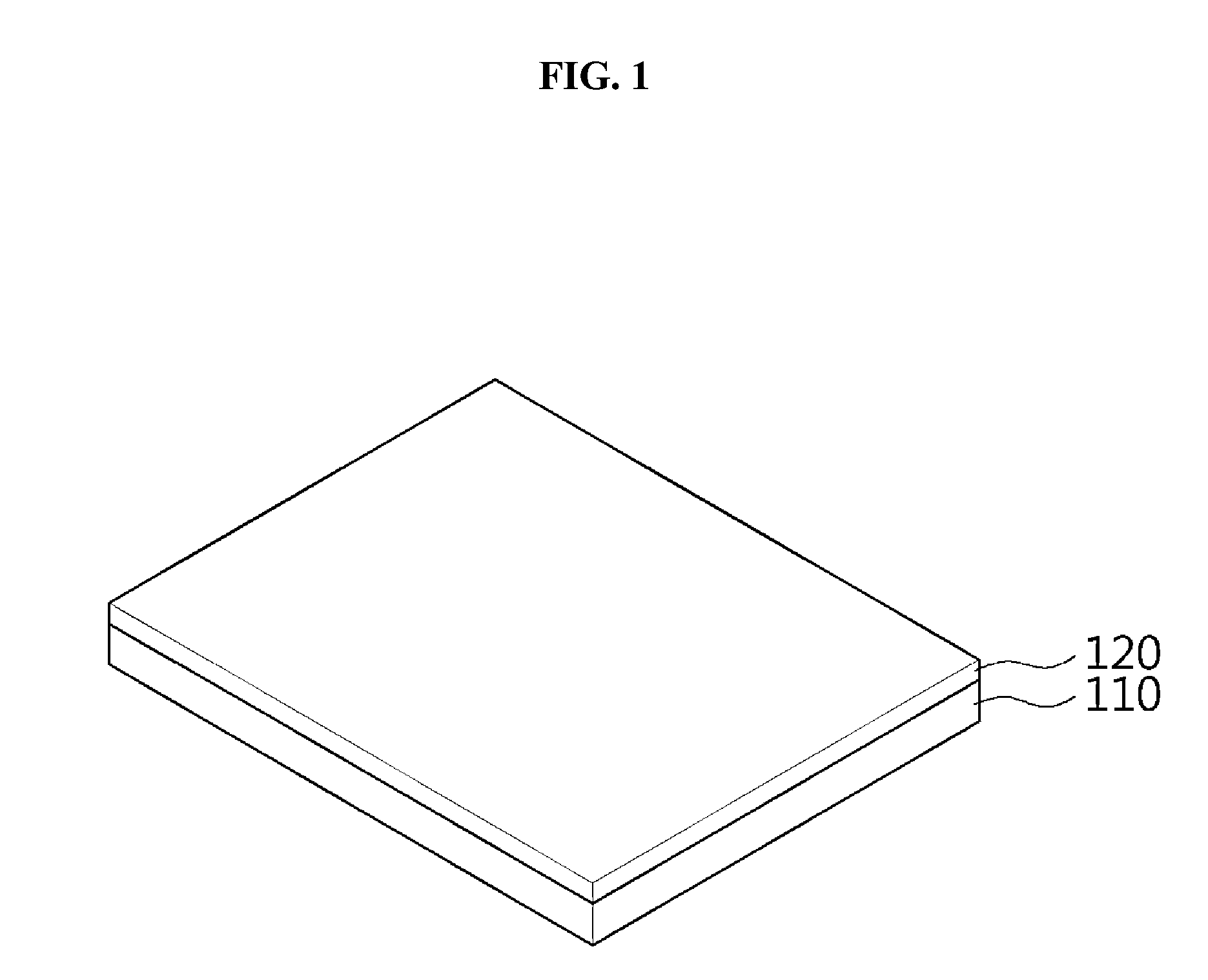
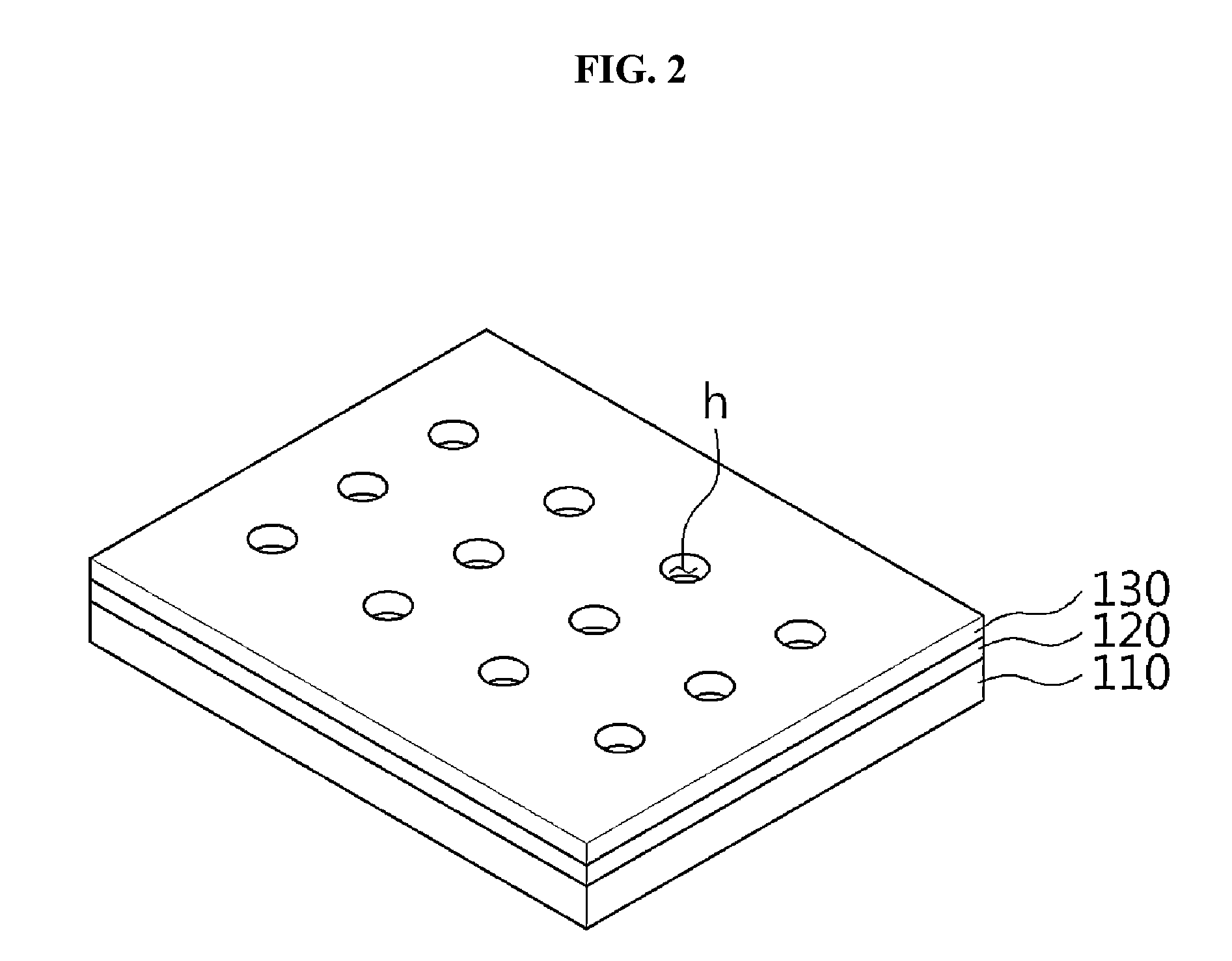
[0044]FIGS. 1 to 6 are perspective views (FIGS. 1 to 4 and 6) and a sectional view (FIG. 5) for explaining the method for fabricating the nanostructure array substrate 100 according to one embodiment of the present invention.

[0045]Referring to FIG. 1, a ZnO seed layer 120 is formed on a substrate 1...

embodiment 2

Fabrication of Nanostructure Array Substrate

[0084]According to one embodiment of the present invention, the nanostructure array substrate is fabricated through the steps of forming a ZnO seed layer patterned in a form of dots on a substrate; forming ZnO nanorods vertically aligned from the ZnO seed layer; and coating a TiO2 sol on the ZnO nanorods and sintering the ZnO nanorods to form nanorods having a ZnO core / TiO2 shell structure.

[0085]According to the present embodiment, different from Embodiment 1, the ZnO seed layer is patterned in the form of dots. That is, the ZnO seed layer is aligned on the substrate in the form of dots spaced apart from each other by a predetermined interval. The ZnO seed layer patterned in the form of dots can be obtained through various schemes.

[0086]FIGS. 7 to 9 are sectional views showing an example of forming the ZnO seed layer patterned in the form of dots on the substrate.

[0087]Referring to FIG. 7, a hydrophobic self-assembled layer 320 and a Zn la...

embodiment 3

Application of Nanostructure Array Substrate in Dye-Sensitized Solar Cell

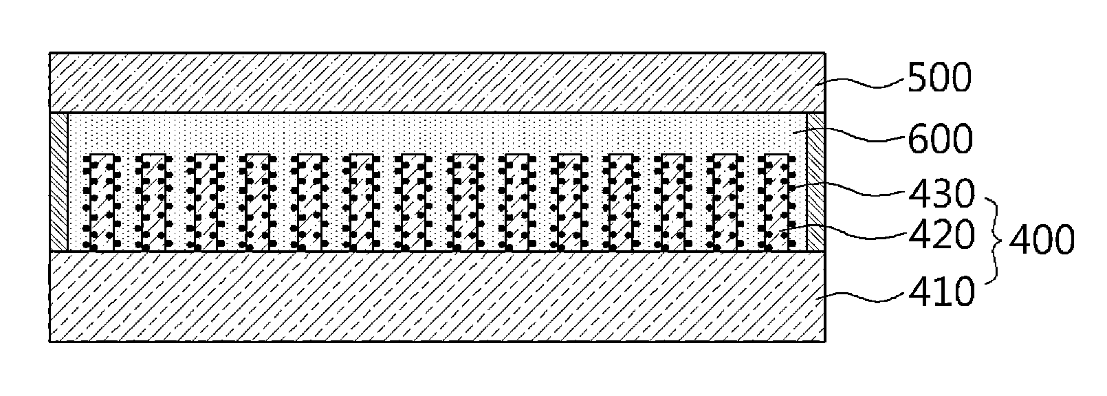
[0101]FIG. 10 is a sectional view schematically showing a dye-sensitized solar cell according to one embodiment of the present invention.

[0102]Referring to FIG. 10, the dye-sensitized solar cell includes a photo electrode 400, a counter electrode 500 opposite to the photo electrode 400, and an electrolyte 600 interposed between the photo electrode 400 and the counter electrode 500.

[0103]The photo electrode 400 includes a transparent conductive substrate 410; a plurality of metal oxide nanostructures 420 vertically aligned on the substrate 410 while being separated from each other; and a dye 430 adsorbed in the metal oxide nanostructures 420, wherein the metal oxide nanostructures 420 include nanorods having a ZnO core / TiO2 shell structure or TiO2 nanotubes.

[0104]The transparent conductive substrate 410 may be identical to the substrate of Embodiment 1. When the dye-sensitized solar cell is driven, the transpare...


PUM


Abstract

Disclosed are a nanostructure array substrate, a method for fabricating the same, and a dye-sensitized solar cell by using the same. The nanostructure array substrate includes a plurality of metal oxide nanostructures vertically aligned on the substrate while being separated from each other. The metal oxide nanostructures include nanorods having a ZnO core / TiO2 shell structure or TiO2 nanotubes. The method includes the steps of forming ZnO nanorods vertically aligned from a seed layer formed on a substrate; and coating a TiO2 sol on the ZnO nanorods and sintering the ZnO nanorods to form nanorods having a ZnO core / TiO2 shell structure. The transparency and flexibility of the substrate are ensured. The photoelectric conversion efficiency of the solar cell is improved if the nanostructure array substrate is employed in the photo electrode of the dye-sensitized solar cell.

Description

CROSS-REFERENCE TO RELATED APPLICATION[0001]This application claims the benefit under 35 U.S.C. §119 of Korean Patent Application No. 10-2011-0070783, filed on Jul. 18, 2011 in the Korean Intellectual Property Office, the entirety of which is incorporated herein by reference.BACKGROUND OF THE INVENTION[0002]1. Field of the Invention[0003]The present invention relates generally to a nanostructure array substrate, a method for fabricating the same, and an application of the same. More particularly, the present invention relates to a metal oxide nanostructure array substrate, a method for fabricating the same, and a dye-sensitized solar cell using the same.[0004]2. Description of the Related Art[0005]The one-dimensional structures having a nano-scale, such as nanorods or nanowires, have inherent optical and electric characteristics, so the one-dimensional structures have been used for various electronic devices and optical devices.[0006]Korean Unexamined Patent Publication No. 2010-008...

Claims


Application Information

Patent Timeline
IPC IPC(8): H01L31/0336H01L21/36H01L29/15B82Y40/00B82Y99/00
CPCH01G9/2031H01G9/2036Y02E10/542H01M14/005H01G9/204B82B1/00B82B3/00H01L31/04
Inventor JUNG, GUN YOUNGSONG, HUIKIM, KI SEOK
Owner GWANGJU INST OF SCI & TECH
Why Eureka
Try Eureka