Package for a MEMS sensor and manufacturing process thereof

Active Publication Date: 2013-02-07
STMICROELECTRONICS MALTA
View PDF4 Cites 37 Cited by
  • Summary
  • Abstract
  • Description
  • Claims
  • Application Information

AI Technical Summary

Benefits of technology

[0016]All the above solutions may be improved in order to better exploit the available space and reduce the general bulk of the package for

Problems solved by technology

This known solution is susceptible of improvements.
In addition, the pitch and layout of the molding and punching tools are not always compatible with the dimensions and configuration of the array of contacts.
Furthermore, this known

Method used


Image

  • Package for a MEMS sensor and manufacturing process thereof
  • Package for a MEMS sensor and manufacturing process thereof
  • Package for a MEMS sensor and manufacturing process thereof

Examples


Embodiment Construction

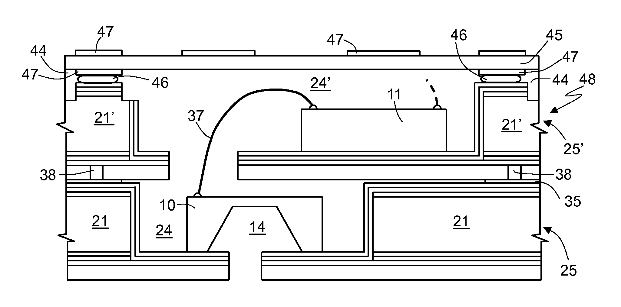
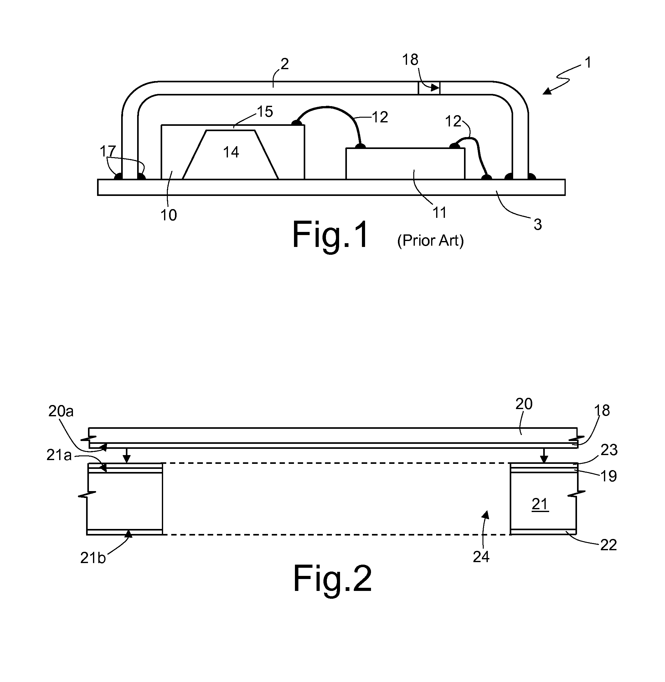
[0027]FIGS. 2-17 show an embodiment of a process for manufacturing a package for a MEMS device and is based on the use of composite substrates that are stacked and bonded to each other. In particular, the following description regards the manufacture of a packaged device through stacking of at least two composite structures, each supporting at least one die, wherein each composite structure may be manufactured basically using the technology described in PCT / EP2010 / 070608 cited above.

[0028]FIGS. 2-17 show only a portion of layers and structures intended to form a single packaged MEMS device, but the same features shown and described repeat on the sides of the illustrated portions, for simultaneous manufacturing the a plurality of packaged MEMS devices.

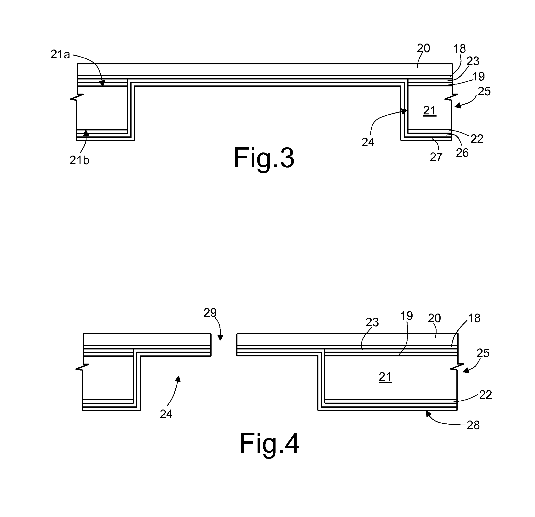
[0029]FIG. 2 shows the coupling of a first and a second package layers 20, 21 (also indicated as a support layer and a wall layer) of a same plastic material, in particular an epoxy resin, and specifically a laminated BT (bismaleimide t...


PUM


Abstract

A packaged MEMS device, wherein at least two support structures are stacked on each other and are formed both by a support layer and a wall layer coupled to each other and delimiting a respective chamber. The chamber of the first support structure is upwardly delimited by the support layer of the second support structure. A first and a second dice are accommodated in a respective chamber, carried by the respective support layer of the first support structure. The support layer of the second support structure has a through hole allowing wire connections to directly couple the first and the second dice. A lid substrate, coupled to the second support structure, closes the chamber of the second support structure.

Description

BACKGROUND[0001]1. Technical Field[0002]The present disclosure relates to a package for a MEMS (Micro-Electro-Mechanical System) sensor, in particular a capacitive microphone, and to the manufacturing process thereof.[0003]2. Description of the Related Art[0004]As is known, a MEMS sensor, e.g., an acoustic transducer such as a capacitive microphone, generally comprises a micromechanical sensing structure, designed to convert a mechanical stress (e.g., acoustic pressure waves) into an electrical quantity (for example, by exploiting variations of the electrical quantity in a capacitive structure of the MEMS sensor due to the acoustic pressure waves), and reading electronics, designed to carry out appropriate processing operations (including amplification and filtering) of the electrical quantity for supplying an electrical output signal (for example, a voltage).[0005]Generally, an MEMS acoustic transducer is formed in a die including a structural layer of semiconductor material, for e...

Claims


Application Information

Patent Timeline
IPC IPC(8): H01L23/12H01L21/50
CPCB81B2207/012H04R19/005B81B2201/0257B81B7/0061H04R2201/003H01L2224/48091H01L2224/48137H01L2224/48227H01L2224/4824H01L2924/00014B81B7/0074B81C1/00309H04R19/04H04R31/00
Inventor FORMOSA, KEVIN
Owner STMICROELECTRONICS MALTA
Why Eureka
Try Eureka