Testing of electroluminescent semiconductor wafers
- Summary
- Abstract
- Description
- Claims
- Application Information
AI Technical Summary
Benefits of technology
Problems solved by technology
Method used
Image
Examples
Embodiment Construction
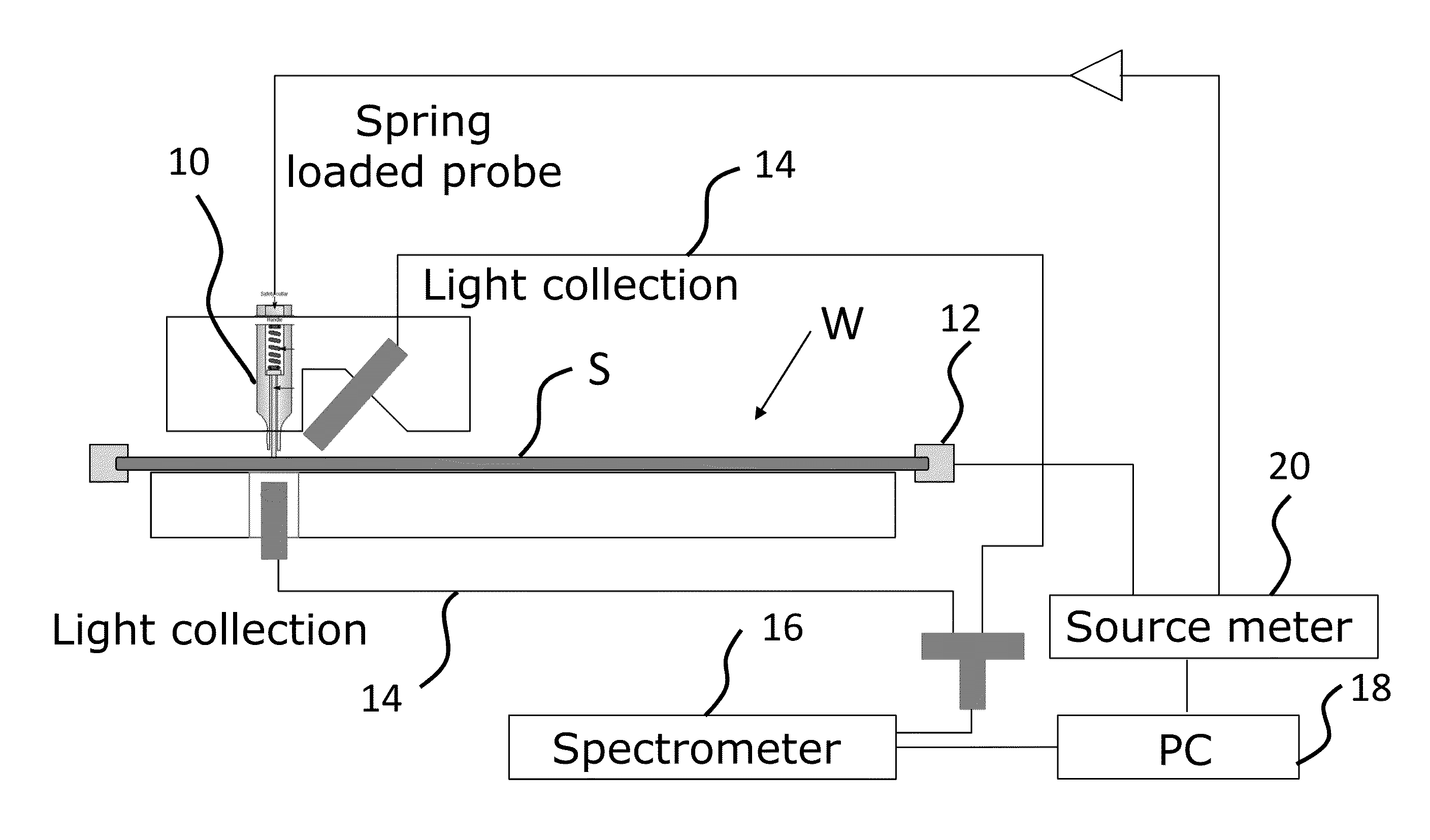
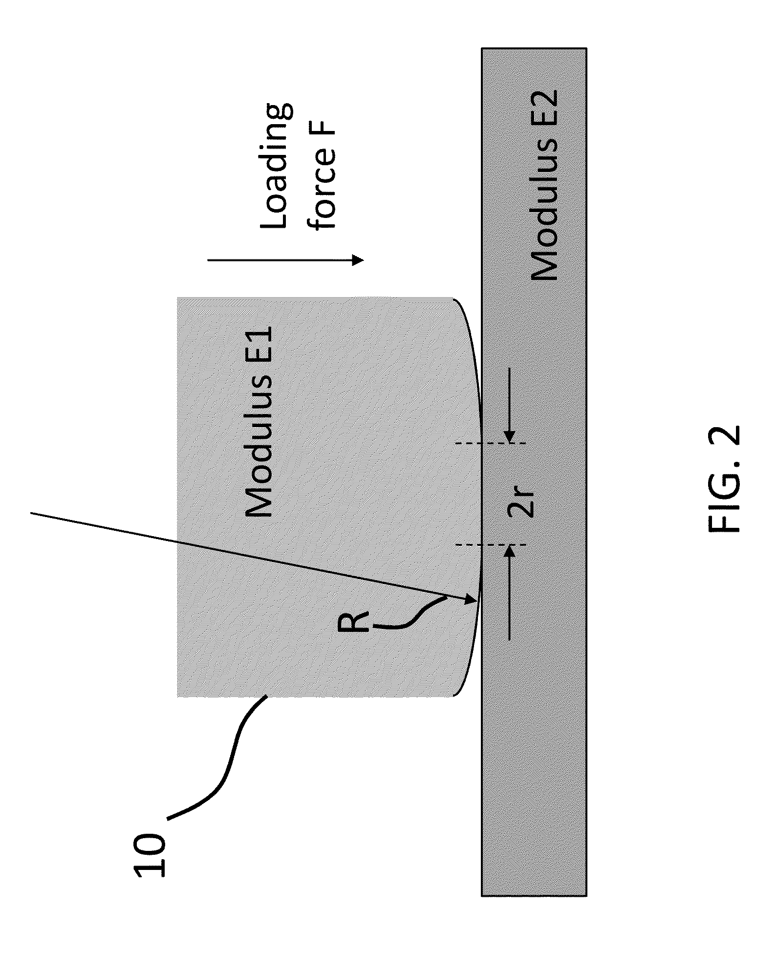
[0021]The invention is described with reference to voltage drift, but it is understood that a corresponding light-intensity drift of the EL semiconductor structure is always associated with a voltage drift. A shaped and polished metal probe is preferred when the light-emitting wafer has a very smooth surface; however, when the wafer has a rougher surface, the conductive polymer material typically used in the art is preferred. Referring to the figures, wherein like parts are referenced with the same numerals and symbols, FIG. 2 shows the conductive probe 10 with a spherical-shape tip used during the development of the present invention. For given probe and wafer materials, the contact area is the function of the loading force F and the radius of curvature R of the probe tip (i.e., the shape of the contact surface). Therefore, by controlling the shape of the probe and the loading force, it is possible to adjust the radius r of the contact area within a range from a few micrometers to ...
PUM
 Abstract
Description
Claims
Application Information


