Pattern inspection apparatus and pattern inspection method

a technology of pattern inspection and inspection apparatus, which is applied in the direction of television systems, semiconductor/solid-state device testing/measurement, instruments, etc., can solve the problems of pattern defect, mask surface deformation, and mask yield drop

Active Publication Date: 2013-02-21
NUFLARE TECH INC
View PDF2 Cites 35 Cited by
  • Summary
  • Abstract
  • Description
  • Claims
  • Application Information

AI Technical Summary

Benefits of technology

[0012]In accordance with one aspect of the present invention, an inspection apparatus includes a stage on which an inspection target object with a plurality of figure patterns formed thereon is placed and which is movable, a light source configured to emit an inspection light, a sensor configured to capture an optical image of the plurality of figure patterns formed on the inspection target object by using the inspection light while moving relatively to the stage, a first image acquisition control unit configured, with respect to a plurality of discrete small regions in a plurality of small regions made by virtually dividing a whole of an inspection region of the inspection target object into strip-like regions, to control so as to acquire an optical image in each of the plurality of discrete small regions in order, while relatively moving the sensor and the stage without performing imaging with respect to a region located between each of the plurality of discrete small regions, a second image acquisition control unit configured to control so as to acquire an optical image in each small region in the whole of the inspection region of the inspection target object in order while relatively moving the sensor and the stage, a first positional deviation amount calculation unit configured to calculate a first positional deviation amount between a dimension of a figure in each optical image acquired when capturing images of the plurality of discrete small regions and a dimension of a figure in a reference image corresponding to the

Problems solved by technology

One of major factors that decrease the yield of the LSI manufacturing is a pattern defect of a mask used when exposing (transferring) a fine pattern onto a semiconductor wafer by the photolithography technology.
If there is no matching between the measurement data and the reference data, it is judged that a pattern defect exists.
Then, during such several hours of mask defect inspection, there occurs a problem in that a pattern position and a pattern dimension obtained based on a measured result vary in the mask surface by a thermal expansion of the mask to be inspected, which is generated from the storage of energy of inspection light irradiated on the mask, by a measurement error of the stage position measuring system, which is generated from a change of air current inside the inspection apparatus or various heat sources in the apparatus, and so on.
Consequently, the uniformity of pattern position accuracy and the uniformity of pattern di

Method used


Image

  • Pattern inspection apparatus and pattern inspection method
  • Pattern inspection apparatus and pattern inspection method
  • Pattern inspection apparatus and pattern inspection method

Examples


embodiment 1

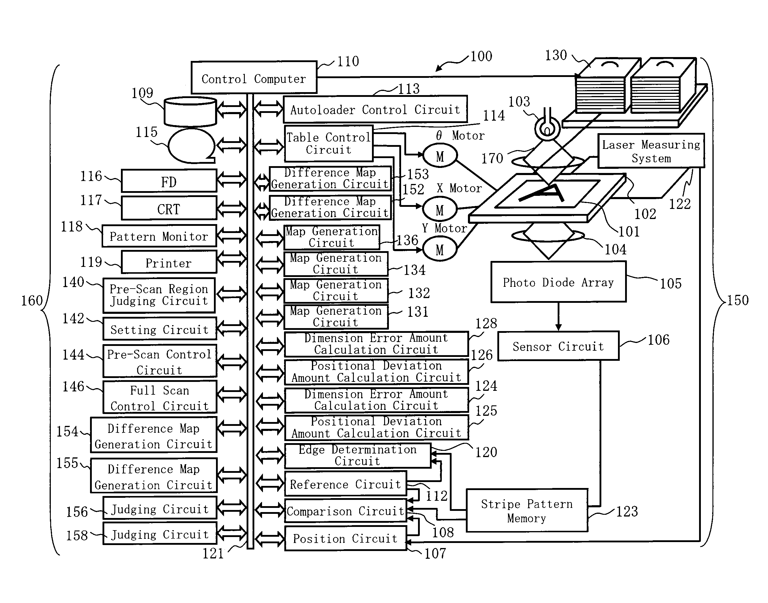
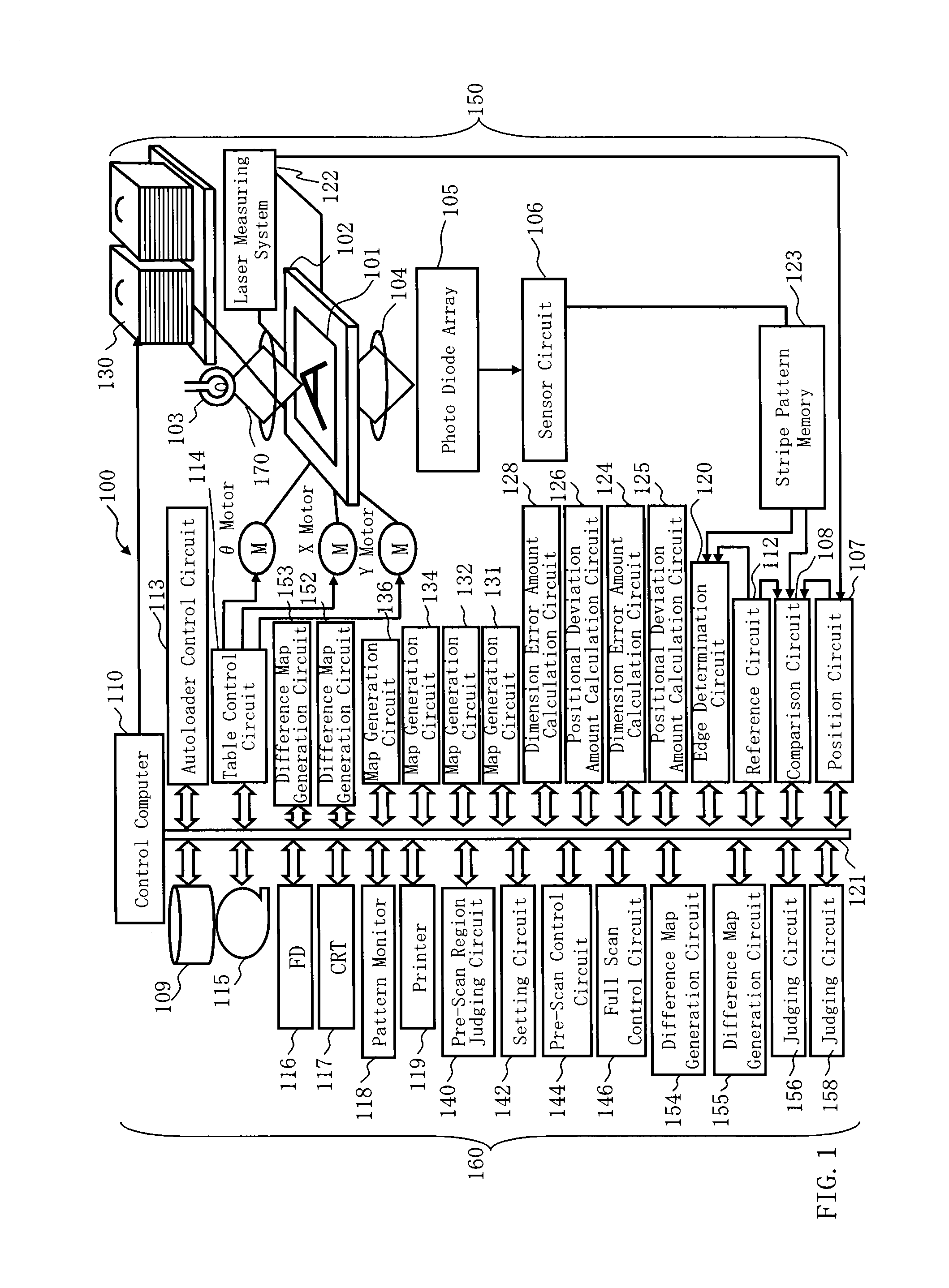
[0027]FIG. 1 is a schematic diagram showing a configuration of a pattern inspection apparatus according to Embodiment 1. In FIG. 1, an inspection apparatus 100 for inspecting a defect of a target object, such as a mask, includes an inspection unit 150 and a control system circuit 160. The inspection unit 150 includes a light source 103, an XYθ table 102, an illumination optical system 170, a magnifying optical system 104, a photo diode array 105 (an example of a sensor), a sensor circuit 106, a stripe pattern memory 123, a laser measuring system 122, and an autoloader 130. In the control system circuit 160, a control computer 110 is connected, through a bus 121, to a position circuit 107, a comparison circuit 108, a reference circuit 112, an autoloader control circuit 113, a table control circuit 114, a magnetic disk drive 109, a magnetic tape drive 115, a flexible disk drive (FD) 116, a CRT 117, a pattern monitor 118, a printer 119, an edge determination circuit 120, positional dev...


PUM


Abstract

A pattern inspection method according to one aspect of the present invention includes generating a first positional deviation amount map by using data acquired by a pre-scan, generating a second positional deviation amount map by using data acquired by a full scan, generating a first positional deviation difference map by calculating a difference between the first positional deviation amount map and the second positional deviation amount map, generating a third positional deviation amount map from the first positional deviation difference map and the second positional deviation amount map, and judging existence of a value exceeding an allowable value, in values defined by the third positional deviation amount map.

Description

CROSS-REFERENCE TO RELATED APPLICATION[0001]This application is based upon and claims the benefit of priority from the prior Japanese Patent Application No. 2011-178877 filed on Aug. 18, 2011 in Japan, the entire contents of which are incorporated herein by reference.BACKGROUND OF THE INVENTION[0002]1. Field of the Invention[0003]The present invention relates to a pattern inspection apparatus and a pattern inspection method. For example, it relates to an inspection apparatus that inspects a pattern by comparing an optical image of a pattern image, which is obtained by irradiating illumination light, with a reference image, which is generated from configuration data etc., and relates to a method therefor.[0004]2. Description of Related Art[0005]In recent years, with the advance of high integration and large capacity of a large scale integrated circuit (LSI), the line width (critical dimension) required for a circuit of a semiconductor element is becoming narrower and narrower. Such s...

Claims


Application Information

Patent Timeline
IPC IPC(8): H04N7/18G06K9/00
CPCG06K9/00H04N7/18G01B11/02G01N21/95H01L22/00G01B2210/56G03F7/70616H01L2924/0002G01N21/95607G01N2021/95615G03F1/84H01L2924/00G06F18/00G03F7/707
Inventor MATSUMOTO, EIJIKIKUIRI, NOBUTAKATSUCHIYA, HIDEO
Owner NUFLARE TECH INC
Why Eureka
Try Eureka