Analog-to-digital converter and wireless receiver

a technology of analog-to-digital converter and wireless receiver, which is applied in the direction of code conversion, pulse technique, instruments, etc., can solve the problems of difficult to provide a low jitter clock at the high frequency of 1 gs/s and sufficiently low power consumption, and difficult to provide an ultrafast and high-resolution analog-to-digital converter

Inactive Publication Date: 2013-03-07
HITACHI LTD
View PDF6 Cites 49 Cited by
  • Summary
  • Abstract
  • Description
  • Claims
  • Application Information

AI Technical Summary

Problems solved by technology

However, it is difficult to correct the influence of a jitter that is a random time deviation of a sampling timing by performing adaptive control using a least mean square (LMS) algorithm because of its random properties.
It is difficult to provide a low jitter clock at the high frequency of 1 GS/s and sufficiently low power consumption.
In other words, under present circumstances, it is difficult to provide an ultrafast and high-resolution analog-to-digital converter because of the jitter included

Method used


Image

  • Analog-to-digital converter and wireless receiver
  • Analog-to-digital converter and wireless receiver
  • Analog-to-digital converter and wireless receiver

Examples


first embodiment

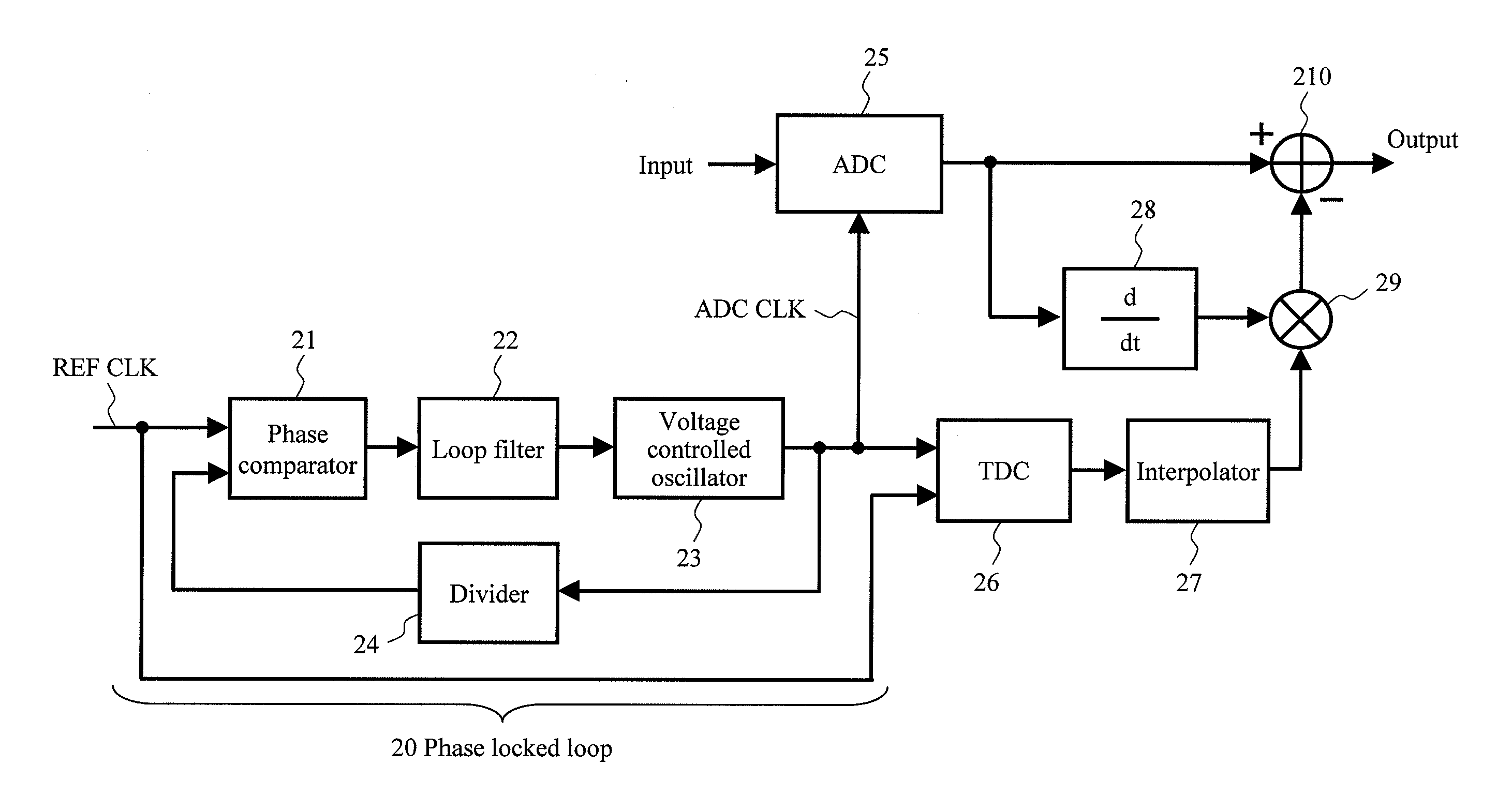
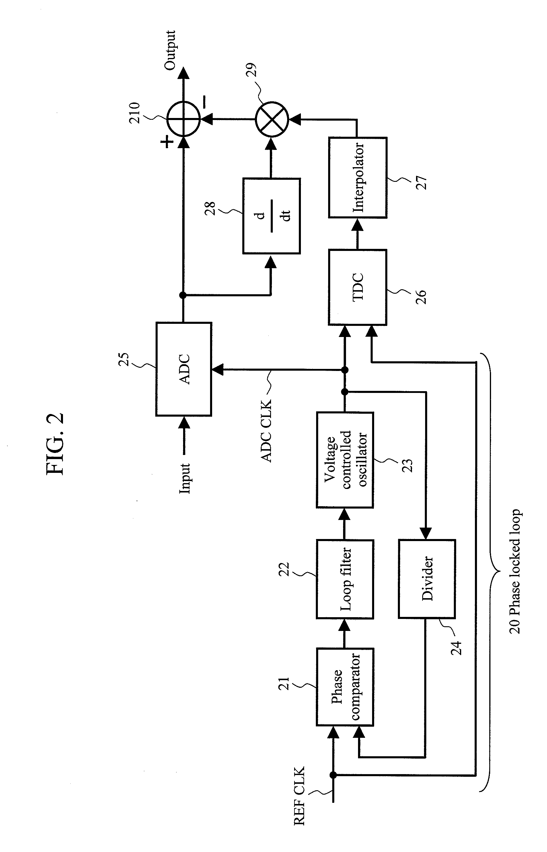
[0049]FIG. 2 shows an example of a structure of an analog-to-digital converter according to a first embodiment. In the first embodiment, a sampling clock (ADC CLK) used in the analog-to-digital converter is generated in a phase locked loop (PLL) 20 using a reference clock (REF CLK) as a source oscillation.

[0050]The phase locked loop 20 includes a phase comparator 21, a loop filter 22, a voltage control oscillator (VCO) 23, a divider 24, and the like. Incidentally, the phase comparator 21 may be a phase frequency comparator, and a charge pump circuit may be provided between the phase comparator 21 and the loop filter 22. Generally, a low-pass filter is used as the loop filter 22.

[0051]The circuit structure of the phase locked loop 20 is commonly known. Accordingly, the phase locked loop 20 performs the normal operation that is commonly known. Specifically, the output of the voltage control oscillator 23 is synchronized with the phase of the reference clock. The output of the voltage ...

second embodiment

[0086]FIG. 8 shows an example of a structure of an analog-to-digital converter according to a second embodiment. The analog-to-digital converter, which has the same circuit structure as in the first embodiment except that the phase locked loop 20 according to the first embodiment is replaced by a circuit structure described later, will be explained in this embodiment. Specifically, the case where the phase locked loop 20 is replaced by a circuit composed of a duty adjustment unit (Duty) 81, a band pass filter (BPF) 82 connected to the output thereof, and a buffer 83 connected to the output thereof will be explained. The structures and operations of the analog-to-digital conversion unit (ADC) 25, the digital correction unit, the time-to-digital converter 26, and the interpolator 27 are the same as in the first embodiment.

[0087]FIG. 9 shows waveforms of outputs from the duty adjustment unit 81, the band pass filter 82, and the buffer 83. FIG. 9 shows the case where the frequency of th...

third embodiment

[0093]FIG. 10 shows an example of a structure of an analog-to-digital converter according to a third embodiment. The analog-to-digital converter, which has the circuit structure as in the first embodiment except that the phase locked loop 20 according to the first embodiment is replaced by a circuit structure described later, will be explained in this embodiment. Specifically, the case where the phase locked loop 20 is replaced by a circuit composed of a duty adjustment unit (Duty) 81, an injection locking oscillator 101 connected to the output thereof, and a buffer 83 connected to the output thereof will be explained. Thus, the structures and operations of the analog-to-digital conversion unit (ADC) 25, the digital correction unit, the time-to-digital converter 26, and the interpolator 27 are the same as in the first embodiment.

[0094]FIG. 11 shows waveforms of outputs from the duty adjustment unit 81, the injection locking oscillator 101, and the buffer 83. FIG. 11 shows the case w...


PUM


Abstract

The influence of a jitter of a sampling clock of an analog-to-digital converter is digitally corrected at low power consumption.
The sampling clock of the analog-to-digital converter is generated by a phase locked loop (PLL) using a reference clock, which has a lower frequency and lower jitter than the sampling clock, as a source oscillation. A time-to-digital converter (TDC) converts a timing error at a timing where the sampling clock and the reference clock are synchronized with each other into a digital value. Incidentally, a timing error at a sampling timing where the reference clock is not present is generated by interpolating a detected timing error. Thus, a jitter value of the sampling clock at each sampling timing is obtained. A sampling voltage error is calculated from the jitter value and the output of the analog-to-digital converter is digitally corrected.

Description

CLAIM OF PRIORITY[0001]The present application claims priority from Japanese patent application JP2011-193965 filed on Sep. 6, 2011, the content of which is hereby incorporated by reference into this application.BACKGROUND OF THE INVENTION[0002]1. Field of the Invention[0003]The present invention relates to an analog-to-digital converter having a digital correcting function and a wireless receiver including the analog-to-digital converter.[0004]2. Background Art[0005]In the field of next-generation industrial altimeter measurement such as a semiconductor inspecting device and a semiconductor manufacturing device and in the field of next-generation wireless communication system such as software radio and cognitive radio, an analog-to-digital converter having a high effective resolution of 10 bits or more and an extremely high conversion rate of 1 GS / s or more is required.[0006]To provide such an ultrafast and high-resolution analog-to-digital converter, various unfavorable characteri...

Claims


Application Information

Patent Timeline
IPC IPC(8): H03M1/50H04L27/00
CPCH03M1/0836H03M1/1215H03M1/12
Inventor OSHIMA, TAKASHINAKAMURA, YOHEI
Owner HITACHI LTD
Why Eureka
Try Eureka