Ultrahigh-speed low-jitter multi-phase clock circuit

A multi-phase clock, low jitter technology, applied in electrical components, electrical pulse generation, automatic power control, etc., can solve problems such as increasing ADC noise floor, increasing ADC spurs, reducing signal-to-noise ratio, etc., to improve performance, Improve clock matching and phase channel count, reduce the effect of sample time mismatch

Active Publication Date: 2017-06-13
BEIJING MXTRONICS CORP +1
View PDF13 Cites 28 Cited by
  • Summary
  • Abstract
  • Description
  • Claims
  • Application Information

AI Technical Summary

Problems solved by technology

Phase jitter will increase the noise floor of the ADC and reduce its signal-to-noise ratio (SNR), while clock skew wil

Method used


Image

  • Ultrahigh-speed low-jitter multi-phase clock circuit
  • Ultrahigh-speed low-jitter multi-phase clock circuit
  • Ultrahigh-speed low-jitter multi-phase clock circuit

Examples


Embodiment Construction

[0051] The present invention will be described in detail below in conjunction with the accompanying drawings and specific embodiments.

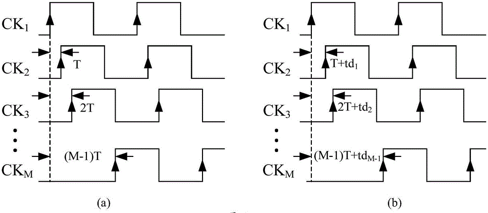
[0052] For an ultra-high-speed low-jitter multi-phase clock system, not only the clock frequency is very high, but also multiple phases are divided into one clock frequency. The time difference between two adjacent phases is already very small. The main difficulty of matching and calibration technology lies in the need The large number of calibrations (related to the number of multi-phase clocks), the calibration accuracy needs to be quite high, and the calibration process needs to be completed in the shortest possible time, all of which pose challenges to the implementation of matching calibration.

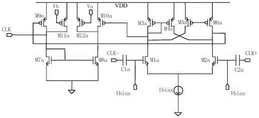
[0053] Such as figure 2 As shown, the present invention provides an ultra-high-speed low-jitter multi-phase clock circuit, which consists of an input clock recovery and duty cycle adjustment module 201, a phase detector module 202, a charge pum...


PUM


Abstract

The invention discloses an ultrahigh-speed low-jitter multi-phase clock circuit. The circuit comprises an input clock recovery and duty ratio adjustment module, a phase discriminator module, a charge pump and loop filter module, a variable delay line module, a clock offset error calibration module and a frequency division module, wherein the phase discriminator module is used for detecting a phase relationship between a reference clock and a feedback clock, and correspondingly outputting an 'UP' or 'Down' pulse level to the charge pump; and the charge pump and a loop filter are used for converting pulses output by a phase discriminator into a low-frequency direct-current control level, and controlling the delay amount of a delay chain to adjust a phase difference between the two clocks; when the two clocks are synchronized, the phase discriminator outputs a locking signal; a variable delay line is constructed by serial connection of a plurality of same sub-delay units in order to obtain a multi-phase clock; and the clock offset error calibration module is used for reducing a clock offset error by adopting a multi-phase clock circuit matching calibration technology. The clock signal can meet strict requirements on clock signals in high-frequency applications.

Description

technical field [0001] The invention relates to a low-jitter multi-phase clock circuit, in particular to an ultra-high-speed low-jitter multi-phase clock circuit for multi-channel time-interleaving analog-to-digital converters, and belongs to the field of integrated circuit clock systems. Background technique [0002] The bandwidth that each semiconductor process can provide is always limited, so the conversion rate of the corresponding analog-to-digital converter is also limited. In order to further increase the conversion rate of the analog-to-digital converter, a time-interleaved operation mode of multiple analog-to-digital converters can be adopted, that is, a time-interleaved analog-to-digital converter (TI ADC: Time Interleaved ADC). Time-interleaved ADC can achieve faster conversion rate with slower technology, so it has always been a research hotspot. This method was proposed by Black and Hodges in 1980, and has been widely studied and applied later. Foreign resear...

Claims


Application Information

Patent Timeline
IPC IPC(8): H03L7/08H03L7/085H03L7/089H03L7/093H03K3/017H03M1/10
CPCH03K3/017H03L7/0807H03L7/085H03L7/0891H03L7/093H03M1/1009
Inventor 薛培帆王宗民张铁良杨松郑迎新崔伟
Owner BEIJING MXTRONICS CORP
Why Eureka
Try Eureka